
Why: a split keyboard many makers build. Its v4 left half brings what no reference circuit has: an RP2040 with its crystal and USB-C port, 23 keys each on a GPIO of its own, and a chain of 23 SK6812MINI-E that runs one diode below 5 V while its data comes from a 3.3 V pin. It is the one LED chain on a board among the designs, and with the v3 it shows the same keyboard without and with a matrix.
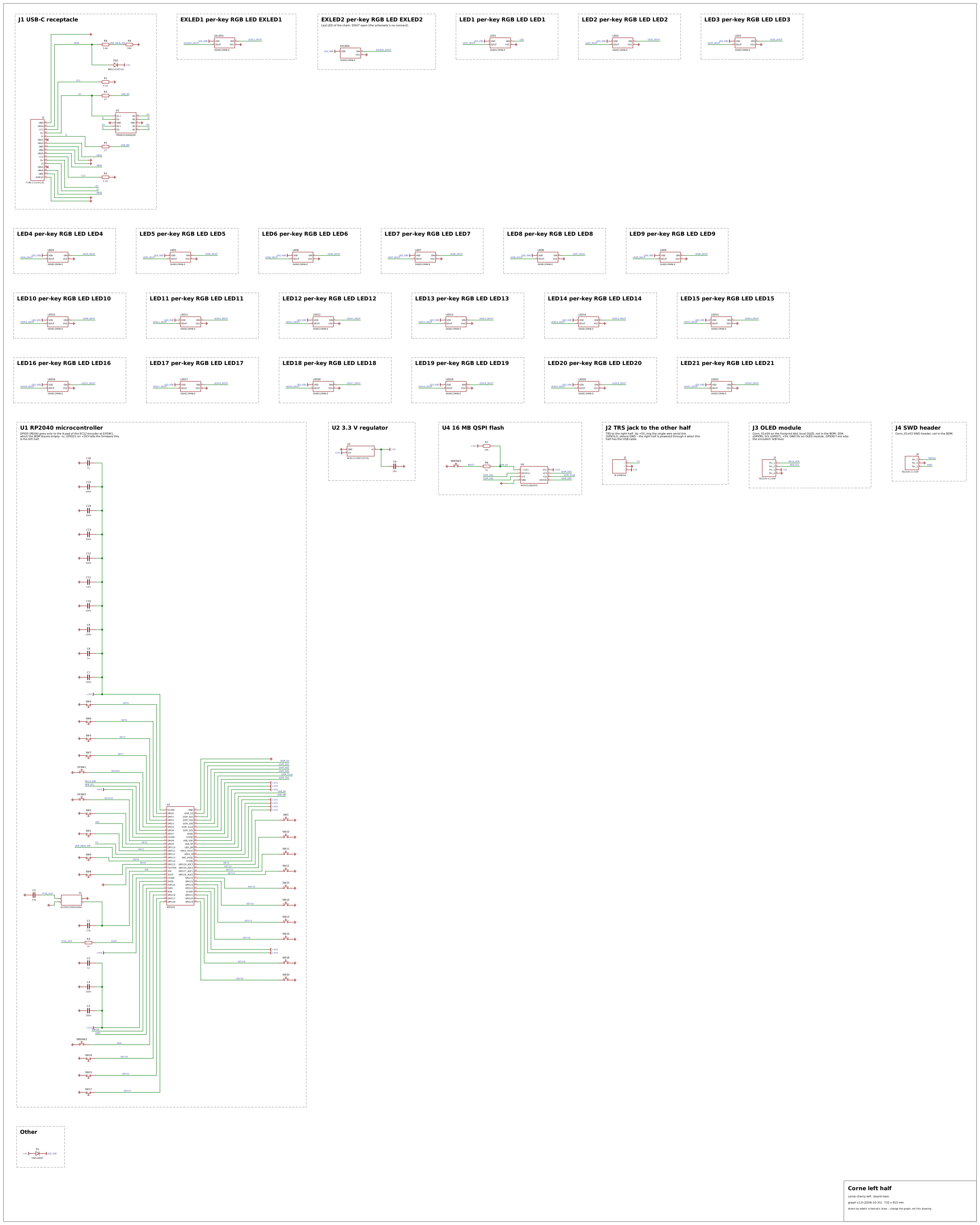
| Stage | Code | Where | Judged | Why |
|---|---|---|---|---|
| check | DOCS.file | edakit.toml | criterion | The transcription has no requirements file: what the published design must do stands in its own documents, not in edakit's form. edakit requires the file before a release (handbook 3.6); it is no point of the design. |
| check | LIM.v | C6 | criterion | The 10 µF / 6.3 V X5R on +5V sees up to 5.25 V – inside its rating, but not with edakit's margin of 1.5 for ceramic capacitors; at 5 V an X5R of 6.3 V keeps only part of its capacitance (DC bias, not read). |
| check | REQ.missing | LED_VDD | real | The 23 SK6812MINI-E have no decoupling capacitor at all; their datasheet calls one at every LED essential (section 14). The chain's supply is one diode below +5V with nothing to buffer the PWM current of 23 LEDs. |
| check | REQ.missing | RE1A_SDA | lacks | The board has no I2C pull-ups; they would have to come from the OLED module the builder plugs into J3, which is not part of the published schematic – whether it brings them depends on the module. |
| check | REQ.missing | REB_SCL | lacks | As RE1A_SDA: a pull-up on SCL can only come from the OLED module, which the schematic does not contain. |
| check | PARTS.supplier | J3 | lacks | J3 is the OLED position, not in the BOM; the 4-pin header that stands in for it has no LCSC number here – LCSC's search refused the request. |
| check | PARTS.verified/device | J3 | lacks | As PARTS.supplier: the stand-in header for the OLED position names neither an LCSC part nor an EasyEDA device. |
| check | REQ.missing/leave | TX | real | The split link runs from GPIO12 straight to the TRS jack's ring – no series resistor, no ESD protection – on a cable that is plugged and unplugged, next to the tip that carries +5V (HINT.jack_supply): a plug pushed in while powered slides the tip's 5 V past the ring contact. |
| sim | LIM.i | J1 | real | With every LED lit at the allowed 70 %, the half draws 0.79 A, beyond the 0.5 A a USB 2.0 port gives – before the right half, which this half also feeds through the jack. The firmware's brightness limit has to keep it below. |
| sim | LIM.i | ZD1 | real | The RB521S30's 200 mA DC rating (160 mA with edakit's derating) carries the whole board: 0.79 A with the LEDs lit, and the right half's current comes on top. |
| sim | LIM.t | ZD1 | real | At 0.79 A the Schottky dissipates far beyond its 200 mW (RθJA 635 °C/W): the LEDs lit at the allowed brightness would destroy it. |
| sim | LIM.t | D1 | real | The 1N4148WT carries the 23 LEDs: 1.31 W at the allowed brightness against 200 mW (RθJA 500 °C/W). Its datasheet gives no continuous current at all, only 300 mA repetitive peak. |
| sim | SIM.state | U2 | real | With the LEDs lit, +5V sags behind the Schottky and the NCP1117LP (dropout about 1.1 V) falls to 2.7–3.2 V. |
| sim | LIM.range | U1 | real | With the LEDs lit at USB nominal or minimum, 3V3 sags below the 3.135 V USB_VDD needs. |
| sim | LIM.range | U4 | real | With the LEDs lit at the lowest USB voltage, 3V3 falls to 2.69 V, below the flash's 2.7 V. |
| sim | LIM.v | C6 | criterion | +5V reaches 4.3–4.9 V against edakit's 67 % derating of the capacitor's 6.3 V (4.22 V) – inside the rating, outside edakit's margin. |
| sim | LIM.range | LED1 | real | One diode (1N4148WT) below +5V – the trick that lifts the RP2040's 3.3 V data above the LEDs' VIH of 0.65 VDD, and the data level passes – the LEDs' VDD is 3.68 V at USB nominal and 3.43 V at the minimum, below the SK6812MINI-E's 3.7 V; with the LEDs lit lower still. |
| sim | LIM.range | LED2 | real | One diode (1N4148WT) below +5V – the trick that lifts the RP2040's 3.3 V data above the LEDs' VIH of 0.65 VDD, and the data level passes – the LEDs' VDD is 3.68 V at USB nominal and 3.43 V at the minimum, below the SK6812MINI-E's 3.7 V; with the LEDs lit lower still. |
| sim | LIM.range | LED3 | real | One diode (1N4148WT) below +5V – the trick that lifts the RP2040's 3.3 V data above the LEDs' VIH of 0.65 VDD, and the data level passes – the LEDs' VDD is 3.68 V at USB nominal and 3.43 V at the minimum, below the SK6812MINI-E's 3.7 V; with the LEDs lit lower still. |
| sim | LIM.range | LED4 | real | One diode (1N4148WT) below +5V – the trick that lifts the RP2040's 3.3 V data above the LEDs' VIH of 0.65 VDD, and the data level passes – the LEDs' VDD is 3.68 V at USB nominal and 3.43 V at the minimum, below the SK6812MINI-E's 3.7 V; with the LEDs lit lower still. |
| sim | LIM.range | LED5 | real | One diode (1N4148WT) below +5V – the trick that lifts the RP2040's 3.3 V data above the LEDs' VIH of 0.65 VDD, and the data level passes – the LEDs' VDD is 3.68 V at USB nominal and 3.43 V at the minimum, below the SK6812MINI-E's 3.7 V; with the LEDs lit lower still. |
| sim | LIM.range | LED6 | real | One diode (1N4148WT) below +5V – the trick that lifts the RP2040's 3.3 V data above the LEDs' VIH of 0.65 VDD, and the data level passes – the LEDs' VDD is 3.68 V at USB nominal and 3.43 V at the minimum, below the SK6812MINI-E's 3.7 V; with the LEDs lit lower still. |
| sim | LIM.range | LED7 | real | One diode (1N4148WT) below +5V – the trick that lifts the RP2040's 3.3 V data above the LEDs' VIH of 0.65 VDD, and the data level passes – the LEDs' VDD is 3.68 V at USB nominal and 3.43 V at the minimum, below the SK6812MINI-E's 3.7 V; with the LEDs lit lower still. |
| sim | LIM.range | LED8 | real | One diode (1N4148WT) below +5V – the trick that lifts the RP2040's 3.3 V data above the LEDs' VIH of 0.65 VDD, and the data level passes – the LEDs' VDD is 3.68 V at USB nominal and 3.43 V at the minimum, below the SK6812MINI-E's 3.7 V; with the LEDs lit lower still. |
| sim | LIM.range | LED9 | real | One diode (1N4148WT) below +5V – the trick that lifts the RP2040's 3.3 V data above the LEDs' VIH of 0.65 VDD, and the data level passes – the LEDs' VDD is 3.68 V at USB nominal and 3.43 V at the minimum, below the SK6812MINI-E's 3.7 V; with the LEDs lit lower still. |
| sim | LIM.range | LED10 | real | One diode (1N4148WT) below +5V – the trick that lifts the RP2040's 3.3 V data above the LEDs' VIH of 0.65 VDD, and the data level passes – the LEDs' VDD is 3.68 V at USB nominal and 3.43 V at the minimum, below the SK6812MINI-E's 3.7 V; with the LEDs lit lower still. |
| sim | LIM.range | LED11 | real | One diode (1N4148WT) below +5V – the trick that lifts the RP2040's 3.3 V data above the LEDs' VIH of 0.65 VDD, and the data level passes – the LEDs' VDD is 3.68 V at USB nominal and 3.43 V at the minimum, below the SK6812MINI-E's 3.7 V; with the LEDs lit lower still. |
| sim | LIM.range | LED12 | real | One diode (1N4148WT) below +5V – the trick that lifts the RP2040's 3.3 V data above the LEDs' VIH of 0.65 VDD, and the data level passes – the LEDs' VDD is 3.68 V at USB nominal and 3.43 V at the minimum, below the SK6812MINI-E's 3.7 V; with the LEDs lit lower still. |
| sim | LIM.range | LED13 | real | One diode (1N4148WT) below +5V – the trick that lifts the RP2040's 3.3 V data above the LEDs' VIH of 0.65 VDD, and the data level passes – the LEDs' VDD is 3.68 V at USB nominal and 3.43 V at the minimum, below the SK6812MINI-E's 3.7 V; with the LEDs lit lower still. |
| sim | LIM.range | LED14 | real | One diode (1N4148WT) below +5V – the trick that lifts the RP2040's 3.3 V data above the LEDs' VIH of 0.65 VDD, and the data level passes – the LEDs' VDD is 3.68 V at USB nominal and 3.43 V at the minimum, below the SK6812MINI-E's 3.7 V; with the LEDs lit lower still. |
| sim | LIM.range | LED15 | real | One diode (1N4148WT) below +5V – the trick that lifts the RP2040's 3.3 V data above the LEDs' VIH of 0.65 VDD, and the data level passes – the LEDs' VDD is 3.68 V at USB nominal and 3.43 V at the minimum, below the SK6812MINI-E's 3.7 V; with the LEDs lit lower still. |
| sim | LIM.range | LED16 | real | One diode (1N4148WT) below +5V – the trick that lifts the RP2040's 3.3 V data above the LEDs' VIH of 0.65 VDD, and the data level passes – the LEDs' VDD is 3.68 V at USB nominal and 3.43 V at the minimum, below the SK6812MINI-E's 3.7 V; with the LEDs lit lower still. |
| sim | LIM.range | LED17 | real | One diode (1N4148WT) below +5V – the trick that lifts the RP2040's 3.3 V data above the LEDs' VIH of 0.65 VDD, and the data level passes – the LEDs' VDD is 3.68 V at USB nominal and 3.43 V at the minimum, below the SK6812MINI-E's 3.7 V; with the LEDs lit lower still. |
| sim | LIM.range | LED18 | real | One diode (1N4148WT) below +5V – the trick that lifts the RP2040's 3.3 V data above the LEDs' VIH of 0.65 VDD, and the data level passes – the LEDs' VDD is 3.68 V at USB nominal and 3.43 V at the minimum, below the SK6812MINI-E's 3.7 V; with the LEDs lit lower still. |
| sim | LIM.range | LED19 | real | One diode (1N4148WT) below +5V – the trick that lifts the RP2040's 3.3 V data above the LEDs' VIH of 0.65 VDD, and the data level passes – the LEDs' VDD is 3.68 V at USB nominal and 3.43 V at the minimum, below the SK6812MINI-E's 3.7 V; with the LEDs lit lower still. |
| sim | LIM.range | LED20 | real | One diode (1N4148WT) below +5V – the trick that lifts the RP2040's 3.3 V data above the LEDs' VIH of 0.65 VDD, and the data level passes – the LEDs' VDD is 3.68 V at USB nominal and 3.43 V at the minimum, below the SK6812MINI-E's 3.7 V; with the LEDs lit lower still. |
| sim | LIM.range | LED21 | real | One diode (1N4148WT) below +5V – the trick that lifts the RP2040's 3.3 V data above the LEDs' VIH of 0.65 VDD, and the data level passes – the LEDs' VDD is 3.68 V at USB nominal and 3.43 V at the minimum, below the SK6812MINI-E's 3.7 V; with the LEDs lit lower still. |
| sim | LIM.range | EXLED1 | real | One diode (1N4148WT) below +5V – the trick that lifts the RP2040's 3.3 V data above the LEDs' VIH of 0.65 VDD, and the data level passes – the LEDs' VDD is 3.68 V at USB nominal and 3.43 V at the minimum, below the SK6812MINI-E's 3.7 V; with the LEDs lit lower still. |
| sim | LIM.range | EXLED2 | real | One diode (1N4148WT) below +5V – the trick that lifts the RP2040's 3.3 V data above the LEDs' VIH of 0.65 VDD, and the data level passes – the LEDs' VDD is 3.68 V at USB nominal and 3.43 V at the minimum, below the SK6812MINI-E's 3.7 V; with the LEDs lit lower still. |
- A crystal with four pads – two ground pads on its lid, the Epson FA-238V at Y1 – stopped edakit check (REQ, pin needs).
- The 12 MHz crystal behind the 1 kΩ damping resistor at the RP2040's XOUT (its datasheet, 2.16, names the damping resistor) taken as missing (REQ.missing).
- A bare microcontroller (kind ic, behaviour mcu) could not state the core current and on-chip regulator the model reads (PARTS.schema).
- Pins on nets no simulated element reaches – the QSPI lines, SWD, the split link – judged as nan against their relative limit (LIM.v/inject, 288 rows).
- The drawing put its no-connect crosses in the order of a set: with two on J1 (SBU1, SBU2) the catalog's SVG changed from run to run.