
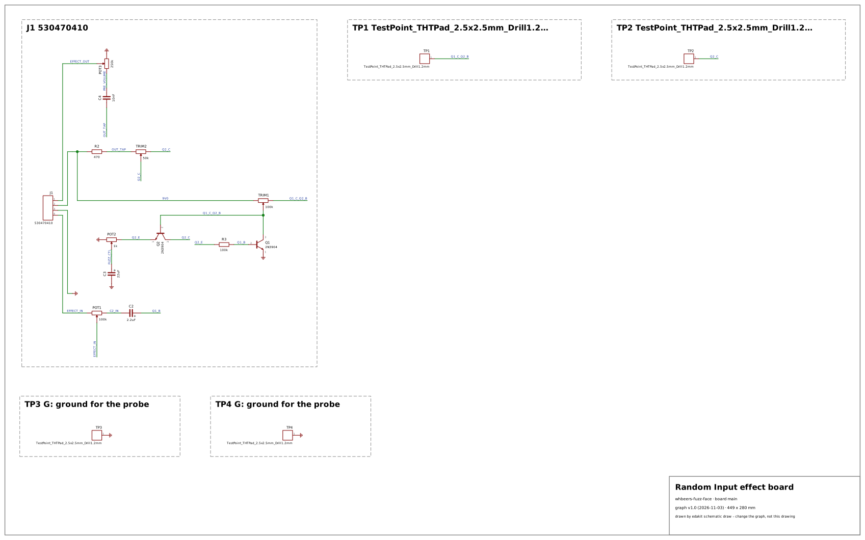
Why: the Fuzz Face is the two-transistor circuit whose bias makers fight with: Q1's collector drives Q2's base directly and Q2's emitter feeds back to Q1's base through 100 kΩ, so the operating point rests on both transistors' gain and leakage – and they pull it in opposite directions, the case of the spread's corners per part (FT-17, handbook 5.2). No reference circuit has a direct-coupled pair, and the open designs' stages are a divider-held common emitter (the Classic Boost) and followers (the combo). This one names its bias targets on the schematic – TP2, Q2's collector, at 5.0 V, TP1 at 500–700 mV – and replaces the collector resistors with trimmers to reach them, so the simulation can hold the bias to the design's own window, show how far the spread moves it at one setting, and show the trimmers' range covering it. It is also a board without an IC, fed through a connector from another board, and its fuzz control carries DC. Makers build the Fuzz Face as one of the first fuzzes: a dozen parts, a sound tied to the transistors, and the reputation for picky bias.
| Stage | Code | Where | Judged | Why |
|---|---|---|---|---|
| check | DOCS.file | edakit.toml | criterion | The transcription has no requirements file: what the published design must do stands in its own documents, not in edakit's form. edakit requires the file before a release (handbook 3.6); it is no point of the design. |
| check | PARTS.verified/device | POT1 | lacks | POT1, the input volume (A100K): the TT Electronics P160 order code that stands in has no LCSC number in the catalogue, and a KiCad design names no EasyEDA device. |
| check | PARTS.verified/device | POT3 | lacks | POT3, the volume (A250K): the TT Electronics P160 with PC pins that stands in has no LCSC number in the catalogue (the solder-lug P160KNP-0QC20A250K, C6249458, has one), and a KiCad design names no EasyEDA device. |
| sim | LIM.v | Q2_C | real | The bias of a Fuzz Face rests on its transistors' gain (FT-17). Trimmed for the typical pair (TRIM2 at 5.05 kΩ: TP2 at 5.0 V), a pair at the low end of the 2N3904's hFE (40) puts Q2's collector at 3.8 V, Q1 at the low end with Q2 at the high end at 3.4 V – outside 4.5–5.5 V; the high end stays inside (5.1 V, Q1 high with Q2 low 5.2 V). Q1 weighs most: its base current through the 100 kΩ feedback sets Q2's emitter. The design's answer is its trimmers and its bias procedure: retrimmed, every pair reaches 5.0 V with TRIM2 between 3.4 and 5.4 kΩ (the extra scenarios 'retrimmed', inside the window). A builder who changes the transistors trims again. |
| sim | LIM.v | Q1_C_Q2_B | lacks | TP1's window, 500–700 mV, is the schematic's for 'medium gain NPN Germanium transistors': no germanium data sheet could be read, the silicon 2N3904 stands in, and with silicon Q1's collector – Q2's base – sits two base-emitter voltages above ground, 1.3–1.6 V over the spread whatever TRIM1 (Q2's emitter must carry Q1's base-emitter voltage through the 100 kΩ). A germanium pair's 0.2–0.3 V junctions put it inside; its spread and leakage need a data sheet the transcription lacks (maker-coverage GTP 1). |
| sim | REQ.value | POT2 | real | The fuzz control POT2 (B1K) is Q2's emitter resistor: Q2's emitter current, 0.66–0.97 mA, flows through its track, and C3 (22 µF) on its wiper sits at half the emitter voltage – 0.33–0.48 V across the half of the track between Q2's emitter and the wiper. Turned while playing, the wiper's step moves C3's charge – the crackle of a control with DC on it (maker-coverage CK-30). It is the circuit's, not this board's: the Fuzz Face's fuzz control is Q2's variable emitter degeneration, 1 kΩ bypassed through its wiper (ElectroSmash's analysis). |
- The test points TP1 to TP4 – the board's plated pads for a wire or a probe asked for an LCSC part or an EasyEDA device (PARTS.verified/device on each): their entry says own.what "copper" now – the board's own, nothing to buy or pick (TD-127).
- TRIM2, Q2's collector trimmer with 3.2–4.9 V across it by design, held to one DC level on both sides like a pot turned while playing (REQ.value/switch): the kind potentiometer had no way to say trimmer. values adjust "trimmer" – the Bourns 3296W entries carry it – leaves it out of the rule (TD-126).
- Q2's base – Q1's collector, held by TRIM1 from 9V0 – judged as floating while 'the firmware is not running' (LVL.undefined): the board has no IC, 9V0 comes in at the connector J1 from the Noise Floor IO board, and no pin types it as a supply. Now the net a source of sim.json feeds (its plus pin) is a rail for the transistors' control pins.