edakit documentation

Corne Cherry keyboard v3, left half

Why: the same keyboard as a real key matrix: 21 keys in a 4 × 6 matrix with a diode per key on a Pro Micro, where the reference circuit keyboard has 2 × 2. edakit's matrix rules and the simulated scan run on it – the scan reads through the diodes and ghosts without them.
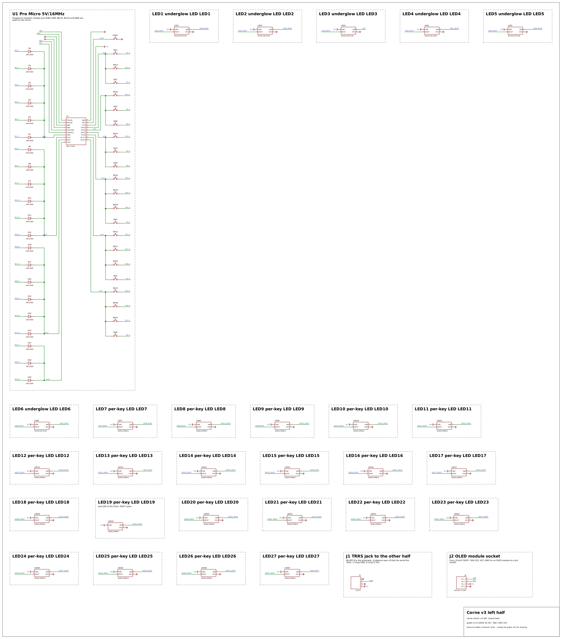
foostan, Corne Cherry v3 (crkbd), https://github.com/foostan/crkbd at commit b473521 (b473521c92c2959997fea41be72e061f3e77797f, 2023-10-18, "Update directory trees", the parent of af19c6d), the schematic corne-cherry/pcb/corne-cherry.kicad_sch ("Corne Cherry", rev 3.0.1, 2020-09-28), read on 2026-10-31 from the git objects of a read-only clone. The sheet holds both halves side by side; transcribed is the half whose nets carry no _r (the right half's are row0_r, col0_r, … on VDD and GNDA) – U1, J1, J2, RSW1, SW1–SW21, D1–D21, LED1–LED27. The netlist was resolved from the schematic by a reader outside this repository and checked against the board file corne-cherry/pcb/corne-cherry.kicad_pcb of the same commit: all 452 pins of the sheet are on the same nets there. The parts follow the build guide corne-cherry/doc/v3/buildguide_en.md of that commit. · SVG

Corne v3 left half corne-cherry-v3-left · board main graph v1.0 (2026-10-31) · 582 x 661 mm drawn by edakit schematic draw – change the graph, not this drawing U1 Pro Micro 5V/16MHz Plugged on headers. Header pins 8/B4, 9/B5, B6/10, B2/16 and RAW are open on the Corne. LED1 underglow LED LED1 LED2 underglow LED LED2 LED3 underglow LED LED3 LED4 underglow LED LED4 LED5 underglow LED LED5 LED6 underglow LED LED6 LED7 per-key LED LED7 LED8 per-key LED LED8 LED9 per-key LED LED9 LED10 per-key LED LED10 LED11 per-key LED LED11 LED12 per-key LED LED12 LED13 per-key LED LED13 LED14 per-key LED LED14 LED15 per-key LED LED15 LED16 per-key LED LED16 LED17 per-key LED LED17 LED18 per-key LED LED18 LED19 per-key LED LED19 Last LED of the chain: DOUT open. LED20 per-key LED LED20 LED21 per-key LED LED21 LED22 per-key LED LED22 LED23 per-key LED LED23 LED24 per-key LED LED24 LED25 per-key LED LED25 LED26 per-key LED LED26 LED27 per-key LED LED27 J1 TRRS jack to the other half MJ-4PP-9 in the schematic: A (sleeve) open, B (tip) the serial link 'data', C (ring) GND, D (ring 2) VCC. J2 OLED module socket Conn_01x04 'OLED': SDA, SCL, VCC, GND for an OLED module on a pin socket. LED LED data data SDA SDA SCL SCL row0 D1_A D1_A D2_A D2_A D3_A D3_A D4_A D4_A D5_A D5_A D6_A D6_A row1 D10_A D10_A D11_A D11_A D12_A D12_A D7_A D7_A D8_A D8_A D9_A D9_A row2 D13_A D13_A D14_A D14_A D15_A D15_A D16_A D16_A D17_A D17_A D18_A D18_A row3 D19_A D19_A D20_A D20_A D21_A D21_A col5 col4 col3 col2 col1 col0 reset LED1_DOUT LED1_DOUT LED2_DOUT LED2_DOUT LED3_DOUT LED3_DOUT LED4_DOUT LED4_DOUT LED5_DOUT LED5_DOUT LED6_DOUT LED6_DOUT LED7_DOUT LED7_DOUT LED8_DOUT LED8_DOUT LED14_DOUT LED14_DOUT LED9_DOUT LED9_DOUT LED10_DOUT LED10_DOUT LED16_DOUT LED16_DOUT LED11_DOUT LED11_DOUT LED12_DOUT LED12_DOUT LED18_DOUT LED18_DOUT LED13_DOUT LED13_DOUT LED20_DOUT LED20_DOUT LED15_DOUT LED15_DOUT LED22_DOUT LED22_DOUT LED17_DOUT LED17_DOUT LED24_DOUT LED24_DOUT LED21_DOUT LED21_DOUT LED25_DOUT LED25_DOUT LED23_DOUT LED23_DOUT LED27_DOUT LED27_DOUT LED26_DOUT LED26_DOUT VCC VCC VCC VCC VCC VCC VCC VCC VCC VCC VCC VCC VCC VCC VCC VCC VCC VCC VCC VCC VCC VCC VCC VCC VCC VCC VCC VCC VCC VCC TX0/D3 1 RX1/D2 2 GND 3 GND 4 2/D1/SDA 5 3/D0/SCL 6 4/D4 7 5/C6 8 6/D7 9 7/E6 10 GND 23 RST 22 VCC 21 F4/A3 20 F5/A2 19 F6/A1 18 F7/A0 17 B1/15 16 B3/14 15 U1 DEV-12640 D1 1N4148W D2 1N4148W D3 1N4148W D4 1N4148W D5 1N4148W D6 1N4148W D10 1N4148W D11 1N4148W D12 1N4148W D7 1N4148W D8 1N4148W D9 1N4148W D13 1N4148W D14 1N4148W D15 1N4148W D16 1N4148W D17 1N4148W D18 1N4148W D19 1N4148W D20 1N4148W D21 1N4148W SW12 SW18 SW21 SW6 SW11 SW17 SW20 SW5 SW10 SW16 SW19 SW4 SW15 SW3 SW9 SW14 SW2 SW8 SW1 SW13 SW7 RSW1 VDD 1 DOUT 2 DIN 4 VSS 3 LED1 WS2812B-V5/W VDD 1 DOUT 2 DIN 4 VSS 3 LED2 WS2812B-V5/W VDD 1 DOUT 2 DIN 4 VSS 3 LED3 WS2812B-V5/W VDD 1 DOUT 2 DIN 4 VSS 3 LED4 WS2812B-V5/W VDD 1 DOUT 2 DIN 4 VSS 3 LED5 WS2812B-V5/W VDD 1 DOUT 2 DIN 4 VSS 3 LED6 WS2812B-V5/W VDD 1 DOUT 2 DIN 4 VSS 3 LED7 SK6812MINI-E VDD 1 DOUT 2 DIN 4 VSS 3 LED8 SK6812MINI-E VDD 1 DOUT 2 DIN 4 VSS 3 LED9 SK6812MINI-E VDD 1 DOUT 2 DIN 4 VSS 3 LED10 SK6812MINI-E VDD 1 DOUT 2 DIN 4 VSS 3 LED11 SK6812MINI-E VDD 1 DOUT 2 DIN 4 VSS 3 LED12 SK6812MINI-E VDD 1 DOUT 2 DIN 4 VSS 3 LED13 SK6812MINI-E VDD 1 DOUT 2 DIN 4 VSS 3 LED14 SK6812MINI-E VDD 1 DOUT 2 DIN 4 VSS 3 LED15 SK6812MINI-E VDD 1 DOUT 2 DIN 4 VSS 3 LED16 SK6812MINI-E VDD 1 DOUT 2 DIN 4 VSS 3 LED17 SK6812MINI-E VDD 1 DOUT 2 DIN 4 VSS 3 LED18 SK6812MINI-E VDD 1 DIN 4 VSS 3 LED19 SK6812MINI-E VDD 1 DOUT 2 DIN 4 VSS 3 LED20 SK6812MINI-E VDD 1 DOUT 2 DIN 4 VSS 3 LED21 SK6812MINI-E VDD 1 DOUT 2 DIN 4 VSS 3 LED22 SK6812MINI-E VDD 1 DOUT 2 DIN 4 VSS 3 LED23 SK6812MINI-E VDD 1 DOUT 2 DIN 4 VSS 3 LED24 SK6812MINI-E VDD 1 DOUT 2 DIN 4 VSS 3 LED25 SK6812MINI-E VDD 1 DOUT 2 DIN 4 VSS 3 LED26 SK6812MINI-E VDD 1 DOUT 2 DIN 4 VSS 3 LED27 SK6812MINI-E ~ A ~ B ~ C ~ D J1 20153 Pin_1 1 Pin_2 2 Pin_3 3 Pin_4 4 J2 PZ254V-11-04P
StageCodeWhereJudgedWhy
checkDOCS.fileedakit.tomlcriterionThe transcription has no requirements file: what the published design must do stands in its own documents, not in edakit's form. edakit requires the file before a release (handbook 3.6); it is no point of the design.
checkLVL.undefinedLEDrealThe LED chain's data input hangs on TX0/D3 alone: the ATmega32U4's port pins are tri-stated while it resets (datasheet 10.2.1), so LED3's DIN floats until the firmware drives it – no resistor holds it.
checkREQ.missingVCCrealThe 27 LEDs on VCC have no capacitor at all – the board has none. The SK6812MINI-E datasheet calls a decoupling capacitor at every LED essential (section 14); the WS2812B-V5/W's says it needs none.
checkREQ.missingSCLlacksThe board has no I2C pull-ups; they would have to come from the OLED module the builder plugs into J2, which the schematic does not contain.
checkREQ.missingSDAlacksAs SCL: a pull-up on SDA can only come from the OLED module, which the schematic does not contain.
checkPARTS.supplierJ2lacksJ2 is the OLED socket, not named in the build guide by part number; the 4-pin header that stands in has no LCSC number here – LCSC's search refused the request.
checkPARTS.verified/deviceJ1lacksThe stand-in for the MJ-4PP-9, SparkFun's 4UCON 20153, has no LCSC number and no EasyEDA device.
checkPARTS.verified/deviceJ2lacksAs PARTS.supplier: the stand-in header of the OLED socket names neither an LCSC part nor an EasyEDA device.
checkPARTS.verified/deviceU1criterionThe Pro Micro is a bought board, ordered from SparkFun (DEV-12640): edakit asks every part for an LCSC number or an EasyEDA device to place it; this design is KiCad, its footprint kbd:ProMicro_v3.
checkREQ.missing/leavedatarealThe split link runs from RX1/D2 straight to the TRRS jack's tip – no series resistor, no ESD protection – on a cable plugged and unplugged next to the ring that carries VCC.
simLIM.iU1realWith every LED lit the half draws 0.93 A from the Pro Micro's USB, beyond the 0.5 A of a USB 2.0 port and of the module's PTC ('VCC: 5V at 500mA') – before the right half, which it also feeds through the jack. The firmware's brightness limit has to keep it below.
simLIM.rangeU1realWith every LED lit at the lowest USB voltage, VCC sags to 4.47 V behind the cable, below the 4.5 V the ATmega32U4 needs for its 16 MHz.

edakit's false alarms on this design, fixed

  • A pressed key of the matrix whose row is not scanned – SW1 and SW2 in the ghost load, their diodes blocking on purpose – judged as a contact starved of its minimum load, 0 µA against the socket's 10 µA (REQ.value/min_load).
  • The rows not scanned could not be released: every output of the mcu config was driven in every load, so a ghost through a released row could not be simulated. A load's gpio level null now leaves the output on its pull-up.