
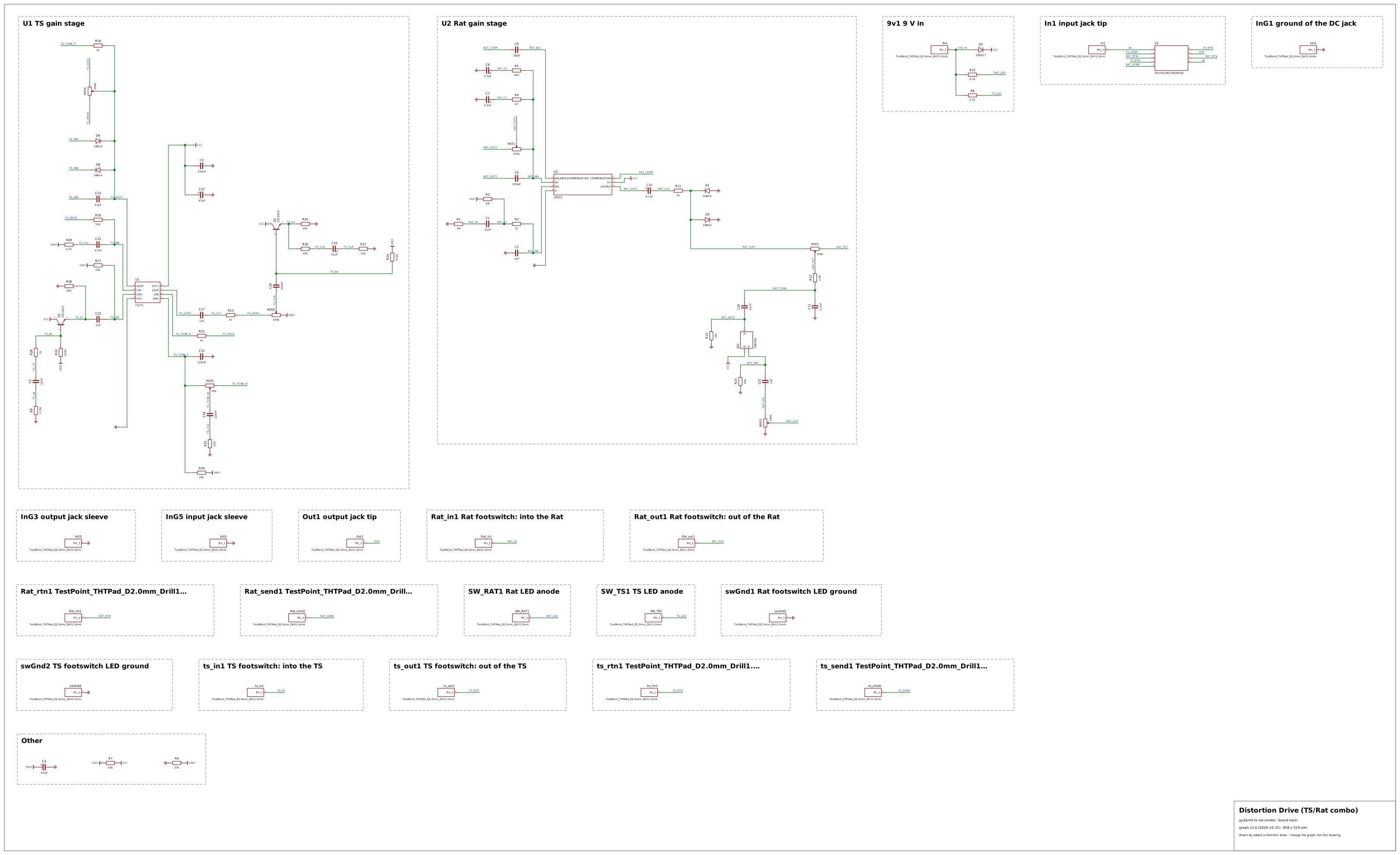
Why: two drive circuits makers copy often, a Tube Screamer-style and a Rat-style stage, on one board: op-amp stages biased at half the supply, BJT and JFET followers, a 3PDT switch on the board that orders the effects, and footswitches wired by hand. It brings real op-amps where the reference circuit guitar has a test entry, and a reversed electrolytic (C19) that edakit finds.
| Stage | Code | Where | Judged | Why |
|---|---|---|---|---|
| check | DOCS.file | edakit.toml | criterion | The transcription has no requirements file: what the published design must do stands in its own documents, not in edakit's form. edakit requires the file before a release (handbook 3.6); it is no point of the design. |
| check | PARTS.verified/device | POT1 | lacks | POT1, the distortion pot, A100K: the TT Electronics P160 order code that stands in has no LCSC number in the catalogue (the B100K of POT6 has one), and a KiCad design names no EasyEDA device. |
| check | PARTS.verified/device | POT2 | lacks | POT2, the filter pot, A100K: the TT Electronics P160 order code that stands in has no LCSC number in the catalogue (the B100K of POT6 has one), and a KiCad design names no EasyEDA device. |
| check | PARTS.verified/device | POT3 | lacks | POT3, the volume pot, A100K: the TT Electronics P160 order code that stands in has no LCSC number in the catalogue (the B100K of POT6 has one), and a KiCad design names no EasyEDA device. |
| check | PARTS.verified/device | POT4 | lacks | POT4, the drive pot, A500K: the TT Electronics P160 order code that stands in has no LCSC number in the catalogue (the B100K of POT6 has one), and a KiCad design names no EasyEDA device. |
| check | PARTS.verified/device | POT5 | lacks | POT5, the tone pot, W20K (stand-in B20K): the TT Electronics P160 order code that stands in has no LCSC number in the catalogue (the B100K of POT6 has one), and a KiCad design names no EasyEDA device. |
| check | PARTS.verified/device | JN1 | lacks | The 2N5458 of onsemi has no LCSC number (the catalogue lists only Central Semiconductor's, whose data sheet is not reachable from here); a KiCad design names no EasyEDA device. |
| check | STRUCT.prefix | SW_TS1 | criterion | SW_TS1 is the schematic's own reference of a wire pad (the LED of a footswitch hangs on it); KiCad does not tie references to kinds, edakit reads SW as a switch. |
| check | STRUCT.prefix | SW_RAT1 | criterion | SW_RAT1 is the schematic's own reference of a wire pad (the LED of a footswitch hangs on it); KiCad does not tie references to kinds, edakit reads SW as a switch. |
| sim | LIM.range | U2 | real | The LM301A runs from VCC, 8.73 V behind the 1N5817 – below the 10 V (±5 V) from which its data sheet specifies it (SNOSBS0D, note 1 of the electrical characteristics). Rats run on 9 V in practice; the data sheet promises nothing there – offset, swing and common-mode range are unspecified. The TL072 beside it is specified from 4.5 V. |
| sim | LIM.v | C19 | real | C19 (10 µF electrolytic, the TS output coupling) sits with its plus – pad 1 of the CP_Radial_D5.0mm footprint, the square pad with the '+' – at ts_out, held at 0 V by R27, and its minus at R26 from Q2's emitter, 3.0–3.4 V: reverse-biased in every state. The schematic draws an unpolarized Device:C, the footprint is polarized. Turned round, the finding goes (tests/test_open_designs.py). |
- The 18 pads for the wires that leave the board – the board's plated pads for a wire or a probe asked for an LCSC part or an EasyEDA device (PARTS.verified/device on each): their entry says own.what "copper" now – the board's own, nothing to buy or pick (TD-127).
- A base biased by resistors – the TS's 2SC1815 followers through 510 kΩ from the divider node VREF – judged as floating while 'the firmware is not running' (LVL.undefined): only a resistor to the emitter or to a net a pin types counted, not ground and not a divider's middle.
- A coupling capacitor in a signal path judged from extreme to extreme of its two nets' ranges – C10 and C19, 8.5 V on one side against −4.5 V on the other, 13 V × 1.5 above their 16 V (LIM.v); its two sides carry the same signal, so like ends are compared.
- Several wires of one net between two boards – the ground to the DC jack, both jack sleeves and both footswitches – stopped the simulation (SIM.converge): the second cable of a net found its ends on different nets.
- The order switch and the footswitches were never judged by REQ.value/switch: their nets run through cables, and the simulation's per-board node names ('IN__main') were looked up among the signal nets.
- A switch of three poles could not be described: the roles of the second and third pole were unknown, the simulation switched only the first, and REQ.value/switch took all nine lugs for one contact.