
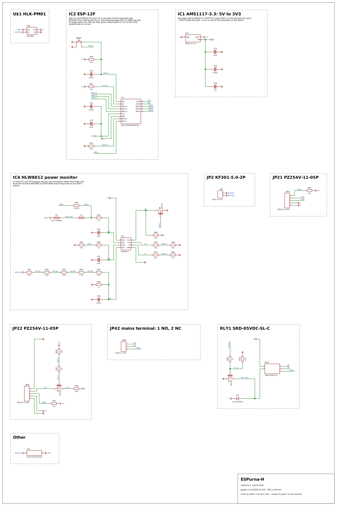
Why: the only board here with mains on it – an HLK-PM01 behind a thermal fuse, a 500 mA fuse and a varistor, a 10 A relay that switches the load, and an HLW8012 power monitor on a 1 mΩ shunt and a 5 × 470 kΩ divider from neutral, whose 0 Ω resistor ties the low-voltage ground to the line. No reference circuit (tests/reference.py has none with mains or a relay) and no other open design brings LIM.hazardous and the domain mains onto a real board, nor a relay coil driven from a 3.3 V GPIO with its flyback diode; around them sit the low-voltage checks edakit does make – the 2N7002's gate drive, the regulator, the ESP8266's levels and boot pins. An HLK-PM01, an ESP module and a relay is the common recipe of a homemade mains smart switch, and ESPurna is a widely used open firmware for such switches, so a false alarm here would meet many.
| Stage | Code | Where | Judged | Why |
|---|---|---|---|---|
| check | DOCS.file | edakit.toml | criterion | The transcription has no requirements file: what the published design must do stands in its own documents, not in edakit's form. edakit requires the file before a release (handbook 3.6); it is no point of the design. |
| check | LIM.hazardous/ground | GND | real | R42 (0 Ω) ties GND to the line behind the shunt R41, as the HLW8012 requires: the ESP-12F, the AMS1117 and the headers JP21 and JP22 – the programming port and the external button – sit at mains potential against earth. edakit holds every range against GND, so none of the low-voltage nets reads hazardous; the ESPurna README warns never to connect the board's ground to a computer while it is on mains. Recognised, not checked. |
| check | LIM.hazardous | NEUTRAL | real | Mains neutral against GND – and GND is the line here (R42): the full mains voltage, 358 V peak at 230 V + 10 %. Recognised, not checked, as edakit means it. The board is meant to sit behind a wall switch in the wall box; the ESPurna README warns never to connect the board's ground to a computer and never to flash it while it is on mains. |
| check | LIM.hazardous | NO | real | The load's line at the terminal JP42: at GND (the line) while the relay is on, pulled to neutral through the load while it is off – hazardous voltage, recognised and not checked. |
| check | LIM.hazardous | NC | real | As NO, the other way round: the changeover contact brought out to JP42.2 carries mains whenever the relay leaves it open. |
| check | LIM.hazardous | V2P_D1 | real | The first tap of the 5 × 470 kΩ divider from neutral to the HLW8012's V2P: four fifths of the mains peak, 286 V. Hazardous voltage on the board, recognised and not checked – its spacing to the low-voltage side is the reviewers'. |
| check | LIM.hazardous | V2P_D2 | real | The divider's second tap, 215 V peak: hazardous voltage on the board, recognised and not checked. |
| check | LIM.hazardous | V2P_D3 | real | The divider's third tap, 143 V peak: hazardous voltage on the board, recognised and not checked. |
| check | LIM.hazardous | V2P_D4 | real | The divider's last tap before V2P, 72 V peak – still above ES1's 60 V. Only V2P itself (0.15 V across R50's 1 kΩ) is below it. |
| check | LIM.v | V11 | real | The S10K250 across the module's input is rated 250 V AC (VRMS, TDK SIOV StandarD series) – its maximum continuous voltage; 230 V + 10 % (EN 50160) is 253 V rms, and edakit's extremes add the line's volt through the fuses: 254 V. A varistor run above its VRMS leaks more and ages; the 275 V types are the usual ones on 230 V mains, and the ESPurna README's own bill of materials names a 270 V varistor. |
| check | LVL.undefined | Q4 | real | Q4's gate hangs on GPIO5 alone, without a pull-down: until the firmware drives GPIO5, SEL is undefined and CF1 may give either quantity. Harmless – the firmware sets SEL before it reads CF1 – but the gate floats, unlike Q3's with R32. |
| check | REQ.missing/leave | GPIO4 | real | The external button's wire (JP22.3) runs straight into GPIO4 – R22 is a pull-up, not in series; a discharge or a short at the wall switch reaches the ESP's pin. |
| check | REQ.value/pin | IC1.4 (VOUT) | real | The AMS1117 datasheet asks for 22 µF (solid tantalum) at the output for stability; the ESPurna-H has 10 µF tantalum (C12) and 100 nF (C21) – 10.1 µF. |
| sim | LIM.range | Q3 | real | GPIO12 drives the relay's 2N7002 through R31/R32 at 3.0 V; its RDS(on) is specified at 5 V and 10 V only, its threshold up to 2.5 V. The model – fitted to the typical part, run at the highest threshold – still pulls the relay in (4.65 V on the coil, 3.75 V needed), but the datasheet does not promise the 71 mA coil current at 3 V: a logic-level MOSFET would. |
| sim | LIM.range | Q4 | known gap | LIM.range/gate (CK-4) finds Q4 half on at VGS 3.3 V. It only pulls SEL low through R49 (0.5 mA): even the part at its highest threshold holds SEL below 1 mV. The rule does not weigh the current, so it warns where nothing burns – as on the SparkFun converter's BSS138. |
- GND tied to the line by R42 unseen: edakit holds every voltage against the board's ground, so the low-voltage side looked safe. LIM.hazardous/ground names a ground joined to a mains terminal's line or neutral (TD-131).
- The module's AC input taken as fed by nothing (PATH.unfed on U$1.1, U$1.2): a connector fed a net only with a vbus role, and marking the terminals reversible would have sent PATH.reverse across the mains side. A connector pin of role line or neutral is a supply input now – JP42.3 and JP2 say so (TD-130).
- The S10K250 (V11) unchecked: edakit had no kind for a varistor, and the transcription entered it as kind ic with behaviour none. The kind varistor holds its VRMS (v_rms_max_v) on AC nets and its VDC (v_max_v) on DC ones – and finds it below 230 V + 10 % (TD-128).
- The mains held as DC: the KF301 terminals' 300 V AC rating and the HLK-PM01's 85 … 265 V AC input against the 358 V peak, and each divider resistor to the highest voltage of its nets against GND (LIM.v on JP2, JP42, U$1.2, R51 to R53). The mains nets are marked ac now, the AC ratings are v_rms_max_v and hold the rms there, and a resistor between two AC nets sees the difference of their like ends – 72 V peak for each of the five (TD-129).
- A need on a regulator's VOUT pin left open while its tab, the same terminal, carries the output: taken as not connected (REQ.missing on IC1.2) instead of judged on the output (REQ.value on IC1.4).