17 Walkthrough on EasyEDA: a coin cell, a button, an LED
If you want to see one whole project before you start your own, this chapter takes a board of four parts – press a button and a red LED lights, from a CR2032 coin cell – from the idea to the delivered boards, in the order things happen. Each step says who does it – you, Claude in a skill, an agent in a session of its own, a command –, which file it writes, what is checked and what came out. The project is examples/coin-cell-led. The short way: the steps.
The outputs are from real runs between 29 and 31 October 2026, shortened where a … stands; the order and the delivered
boards (17.12) are described, not shown.
A finding names its code: the engine that found it and the relation it checks – PATH.reverse the paths a reversed cell
takes, SIM.state what the simulation expects (chapter 14). edakit explain <code> gives the rule, why it exists and
its sources. The release's manual checks keep their numbers, M-1 to M-6 (8.2).
17.1 The steps at a glance
| Step | Who | How | Writes | Checked by | |
|---|---|---|---|---|---|
| 1 | Set up | you answer, Claude writes | /edakit:new-project |
edakit.toml, the graph with its purpose, sim.json, signoff.json, the decision log |
– |
| 2 | What it must do | you and Claude | /edakit:requirements |
hardware/requirements.toml |
DOCS.ref to DOCS.derived |
| 3 | Parts | Claude: the skill part-search or the agent part-selector | edakit part search, part import, part fetch |
hardware/parts/*.json |
STRUCT.entry, STRUCT.identity, PARTS.verified |
| 4 | Circuit | Claude as the circuit designer | /edakit:circuit-design, edakit block add |
hardware/graph.json, hardware/sim.json |
edakit check, edakit sim |
| 5 | What the checks found | Claude proposes, you decide | – | graph, sim.json, decisions D-2, D-3 | the same |
| 6 | Stock and cost | Claude | edakit stock, cost, order |
hardware/stock.json |
PARTS.stock |
| 7 | Drawing and hand-over | Claude | edakit schematic draw, edakit handover |
hardware/schematic.toml, the graph's layout |
SYNC.plan, later |
| 8 | Reviews | the agents electrical-reviewer and regulatory-reviewer, each in a session of its own | – | hardware/signoff.json: M-1, M-6 |
– |
| 9 | The gate offline | Claude | edakit gate |
build/release/<run>/ |
P, G, E |
| 10 | EasyEDA project | you, once; on KiCad edakit writes it (chapter 16) | File → New → Project | – | – |
| 11 | Layout | Claude as the PCB designer, in a session of its own | /edakit:pcb-round |
hardware/boards/main.toml |
pcb plan, route check, round reviews |
| 12 | Release | Claude | edakit gate --eda |
the manufacturing files | P to F, M-5 |
| 13 | Order | Claude up to the maker's cart, you order and pay | edakit cart, /edakit:cart |
the order record hardware/orders/ |
ORDER.form to ORDER.review, M-2 |
| 14 | Acceptance | you | the boards in your hand | – | M-4 |
Steps 1 to 9 work from the files alone – checks, simulation, drawing –, without an EDA program; a board on a breadboard would end there.
17.2 Set up
/edakit:new-project coin-cell-led main asks its questions in one round, a form with options in Claude Code. The
answers here: a PCB, one board main, drawn in EasyEDA Pro, the default (KiCad, the other choice, in chapter 18), made
by JLCPCB with one side assembled, SMD parts only (Economic), 5 sets, no budget, built for oneself in the EU, the
requirements now, no firmware, no documents that quote values, no project scripts or agents. The skill proposes every
file and key with the answer behind it and writes after your OK:
[project]
name = "coin-cell-led"           # EasyEDA project (friendly name); created by hand once, edakit never creates it
company = "edakit example"       # schematic title block
quantity = 5                     # boards per order: the stock check (PARTS.stock) needs this many sets
requirements = "hardware/requirements.toml"   # what the circuit must do (handbook 3.6)

[boards.main]
title = "Coin cell LED"          # page name of the readable schematic; EasyEDA documents and board file by default:
                                 # generated_main, layout_main, PCB main, hardware/boards/main.toml

[release]
assembly = { sides = ["top"], smd_only = true }   # Economic PCBA: one side, SMD only (SYNC.cpl)
The graph starts empty, with what the board is for: "purpose": {"use": "private", "market": "EU", "notes": "…"}. The
purpose decides how deep the regulatory review M-6 goes (chapter 15). That review is support, not legal advice: it
claims no correctness, and nothing in it is legally guaranteed. The answers become decision D-1 in docs/decisions.md.
In a repository of its own the skill also writes the pre-commit hook (edakit check and edakit sim on every commit
that touches hardware/), .gitignore (build/) and .claude/settings.json, which gives every session the plugin.
17.3 What it must do
/edakit:requirements turns the idea into needs – who wants what, in their words – and requirements (3.6): one
statement each, as you state it, and what tests it. It asks back until vague words are your numbers ("lights" becomes
1 mA, "a used cell" 2.5 V, the end voltage Rayovac rates the CR2032's capacity to):
[[requirement]]
id = "R-1"
text = "While SW1 is pressed, D1 carries at least 1 mA – from a fresh CR2032 down to one used to 2.5 V."
source = "N-1; Rayovac rates the CR2032's capacity down to 2.5 V (sim.json, cell 'used')"
from = ["N-1"]
binding = "must"
verify = [{ rows = "SIM.state * D1 LED on" },
          { accept = "press SW1 with a fresh cell: D1 lights; let go: D1 is dark" }]
status = "draft"
R-2 asks that D1 is dark and the cell idle while nobody presses – still without a number, which the reviews (17.9) find.
Claude writes drafts, and every edakit check warns about them (DOCS.draft) until you set status = "accepted"; only
you do. edakit req R-1 shows the chain:
R-1  requirement, must, accepted – hardware/requirements.toml
  source  N-1; Rayovac rates the CR2032's capacity down to 2.5 V (sim.json, cell 'used')
  from    N-1  need, accepted: Press the button and the LED lights; let go and it is dark.
  text    While SW1 is pressed, D1 carries at least 1 mA – from a fresh CR2032 down to one used to 2.5 V.
  verify  rows SIM.state * D1 LED on
          accept press SW1 with a fresh cell: D1 lights; let go: D1 is dark
          not evaluated here – edakit req shows verify as written; the gate evaluates it (section 11 of its protocol)
The rows are simulation results the gate evaluates (8.7); the acceptance step lands on the list for the delivered boards (17.12).
17.4 Parts
Every part needs an entry in the parts database before it goes into the graph (working rules, 3.4). JLCPCB's catalogue knows part words, not function words:
$ edakit part search "CR2032 holder"
JLCPCB catalogue, "CR2032 holder", 2026-10-29: no hits, 4 C99… numbers dropped (user libraries, nobody sells them)
$ edakit part search "CR2032"
JLCPCB catalogue, "CR2032", 2026-10-29: 25 hit(s)
C70373     CR2032Bent Battery Contact Copper 3V  Q&J                     Extended     25013  - – Battery connector
C70377     CR2032-BS-6-1                         Q&J                     Extended     22494  - – Battery connector
C22363833  CR2032-BS-6                           Lian Xin Technology     Extended     15280  SMD – Button And Strip …
…
part import writes the entry from EasyEDA's library – pin numbers and names, footprint, class – and caches symbol and
footprint for the checks; part fetch keeps the datasheet beside the project:
$ edakit part import C70377
hardware/parts/C70377.json: new entry – CR2032-BS-6-1 (QIJEY), footprint BAT-TH_CR2032-BS-6-1, Extended Part, 2 pins
  kind, pin types and roles, values and ratings are for whoever signs it off against its datasheet (handbook 4.3; …)
  library geometry: build/edakit/footprints/BAT-TH_CR2032-BS-6-1.json (2 pads, 33.0 x 16.3 mm)
  symbol: build/edakit/library/C70377.json – STRUCT.entry compares the graph with it
$ edakit part fetch C70377
C70377 CR2032-BS-6-1
  LCSC product data: no pdfUrl
  JLCPCB catalogue https://wmsc.lcsc.com/wmsc/upload/file/pdf/v2/lcsc/1811061923_Q-J-CR2032-BS-6-1_C70377.pdf: PDF behind
    the page's link https://datasheet.lcsc.com/datasheet/pdf/13f0f5570aed4b49bc6fd2928f41a905.pdf?productCode=C70377
  build/edakit/datasheets/C70377.pdf: 838 kB, 1 pages, text layer, sha256 760a7d67242a…
  NOTE    the text does not name CR2032-BS-6-1 – some vendors never print it; compare package, drawing and values with …
The library calls the holder's pins 1 and 2; which is plus, the datasheet says. Its drawing puts "+" at one pad, and
the library footprint draws "+" beside pad 1 on a document layer – pin 1 is plus. Signing the part off (4.3) writes
kind, roles and what was checked against which file; until then PARTS.verified holds the release (17.5):
"kind": "battery_holder",
"pins": {"1": {"name": "1", "type": "passive", "role": "plus"},
         "2": {"name": "2", "type": "passive", "role": "minus"}},
"verified": {"by": "Claude (skill part-search)", "date": "2026-10-29",
             "datasheet": "Q&J QJ.BS-6 battery holder drawing, 2011-02-14",
             "datasheet_sha256": "760a7d67242a4548921d0d92e6f948c3aba7af8ed522d9fdf43bfe59c597a88f",
             "checked": ["pin 1 plus, pin 2 minus: the drawing's PCB layout and the document layer of the library …",
                         "two SMD tabs, no hole: JLCPCB places it on the top side (Economic)"],
             "open": [{"text": "BT1 turned by 180° swaps plus and minus: its orientation in JLCPCB's assembly preview",
                       "when": "order"}]}
An open point with when lands on the checklist of that phase (8.2) – this one is looked at in JLCPCB's preview,
before paying. The push button, the resistor and the LED come with checked entries from edakit's block library.
17.5 Circuit
/edakit:circuit-design reads the requirements instead of asking for them. The cell and the button go into the graph
by hand; the LED with its resistor is the block led:
$ edakit block add led --as LED --connect in=LED_SW
Added block led as LED:
  R1    C17471    150      LED: LED series resistor
  D1    C2297     green    LED: LED (green 0805)
  net LED_SW (exists) + R1.1
  net GND (exists) + D1.2
  net LED_ANODE (new, v [0, 3.3]): R1.2, D1.1
  parts entries copied from the block library: C2297, C17471
The simulation config gets two cell states and two loads, the button pressed and released – the values from the datasheets, an assumption marked as one:
"cells": {
  "fresh": {"v": 3.2, "r": 20,
            "note": "off-load voltage of a fresh CR2032 at least 3.20 V (…); internal resistance at most 20 Ohm …"},
  "used": {"v": 2.5, "r": 40,
           "note": "Rayovac rates the capacity down to 2.5 V (220 mAh at 15 kOhm); 40 Ohm assumed – …"}
},
"supplies": {"fresh": {"BT1": "fresh"}, "used": {"BT1": "used"}},
"loads": {
  "pressed": {"about": "SW1 held down", "buttons": ["SW1"], "leds_on": ["D1"]},
  "released": {"about": "nobody presses", "leds_on": []}
},
"corners": ["min", "max"]
The checks
Then the check loop, seconds a run. edakit check runs the rules over graph and parts (rule checks, 3.3), grouped by
code – stage, place, what against what, and the fix:
$ edakit check
domains: core, power (suggested by the graph – edakit domains)
PATH.reverse – reverse polarity blocked: 1 error
  G  R1.1 on LED_SW: a reversed source reaches this pin without a blocking device   (catalog/paths.toml [reverse]) …
PARTS.verified – parts signed: 1 pending
  P  C70377 CR2032-BS-6-1 (BT1) not verified against its datasheet
DOCS.draft – draft not approved: 4 warning
  G  N-1: a draft – the user has not approved it (status "accepted", or "dropped" with a reason)
  …
HINT.bulk – bulk capacitor at the power input: 1 note
  G  BT1: bulk capacitor at the power input
HINT.lithium – lithium cells need protection: 1 note
  G  BT1: lithium cells need protection
PARTS.stock – parts orderable: 1 note
  P  no stock snapshot (hardware/stock.json) – edakit stock asks JLCPCB about the 4 assembled parts

What to do (edakit explain <code> for rule, why and sources):
  PATH.reverse: A Schottky diode in series, or a PMOS in the supply path with its gate to ground (block reverse-pmos).
  …
not checked for lack of data: LIM.t 2 parts – edakit check --coverage
4 components, 4 nets, 4 parts entries; 1 error, 1 pending, 4 warning, 3 note; requirements: 2 needs, 2 requirements
The first line names the rule sets that are on: core always, power because the graph has a battery holder (the key
[project] domains fixes the list, 10.1). The two HINT notes are design hints, patterns that need judgement rather than
a number. The last line but one names what went unchecked for lack of data: edakit check --coverage says that the
entries of D1 and R1 have no thermal resistance, so no junction temperature is computed (LIM.t). What they carry and
dissipate is checked against their ratings all the same.
The simulation
edakit sim runs every scenario through ngspice (chapter 5):
scenario                           status      VBAT   LED_SW LED_ANODE   supply current
fresh/pressed/vf-min               ok        3.126V   3.126V   2.573V
fresh/pressed/vf-max               ok        3.175V   3.175V   2.991V
fresh/released/vf-min              ok        3.200V   0.000V   0.000V
fresh/released/vf-max              ok        3.200V   0.000V   0.000V
used/pressed/vf-min                fail      2.484V   2.484V   2.424V
used/pressed/vf-max                fail      2.500V   2.500V   2.500V
used/released/vf-min               ok        2.500V   0.000V   0.000V
used/released/vf-max               ok        2.500V   0.000V   0.000V

92 comparisons: fail 2, pass 90

SIM.state – the circuit does what the scenario expects: 2 error
  E  [used/pressed/vf-min] D1: LED on: 0.0003974 A, expected ≥ 1 mA
  E  [used/pressed/vf-max] D1: LED on: 1.166e-07 A, expected ≥ 1 mA
The column "supply current" is for the connectors of sources; a cell's current is not shown, and for R-2 the row "D1
dark" stands in – D1 is the only path.
17.6 What the checks found
Nothing goes on before every finding is fixed or accepted with a reason (working rules, 3.4). Each decision gets its number.
D-2: a red LED
The block's LED stays dark on a used cell (SIM.state). A green LED needs 2.6 to 3.1 V – as much as a used CR2032 has left. A red one needs 1.5 to 2.6 V at 20 mA:
$ edakit part search "LED red 0805" --basic
JLCPCB catalogue, "LED red 0805", 2026-10-29: 1 hit(s)
C84256  NCD0805R1  Foshan NationStar Optoelectronics  Basic   2700112  0805 – LED Indication - Discrete
Its symbol numbers the pins the other way round – pin 1 is the cathode, called -. Changing only the LCSC number in
the graph is caught at once:
STRUCT.entry – graph pins = parts entry: 2 error
  P  D1: pins differ from the library symbol of C84256 (build/edakit/library/C84256.json): pin 1: symbol '-', graph
     'A'; pin 2: symbol '+', graph 'K'
  P  D1: pins differ from parts entry C84256: graph {'1': 'A', '2': 'K'} vs parts {'1': '-', '2': '+'} – the library
     symbol agrees with the entry: the graph has the pins of another part
STRUCT.entry's fix advises per case, by the words the finding starts with. For "pins differ from parts entry" it is the part number of the part whose pins the graph has, or – to keep the red LED – its pin names and the nets on its pins swapped to the entry's.
With the pins and nets swapped, the block's 150 Ω stay. The simulation gives 1.22 mA from a used cell into the LED at
its highest forward voltage, 10.7 mA from a fresh cell at its lowest. LIM.i allows 20 mA, 80 % of its 25 mA; LIM.p holds
the 14.75 mW it then dissipates (Vf × If) to 32.5 mW, half its 65 mW. The computation is in R1's notes, the reason in
D-2.
D-3: a cell upside down
The holder takes the cell either way round, and PATH.reverse wants a blocking part behind it. A Schottky diode in series costs about 0.3 V, the margin R-1 needs from a used cell; a P-MOSFET costs two parts on a board without an IC. The LED blocks by itself, so the finding is accepted on the net with the reason (in full in the graph):
{"name": "LED_SW", "pins": ["SW1.3", "R1.1"], "v": [-3.3, 3.3],
 "accept": {"PATH.reverse": "a cell upside down drives R1 and D1 backwards: D1 blocks, 3.2 V against its VR of 5 V – …"}}
The simulation shows that the reason holds: a cell state reversed (−3.2 V) and an extra scenario with the button
pressed. Its first run failed: the nets were declared from 0 V, and a reversed cell is part of the worst case v
describes (conventions, 3.2):
reversed/pressed                   fail     -3.200V  -3.200V  -3.200V

104 comparisons: fail 3, pass 101

LIM.declared – net inside its declared range: 3 error
  E  [reversed/pressed] VBAT: net voltage inside the declared range: -3.2 V, expected 0 … 3.3 V   (v of net VBAT …)
  …
With VBAT, LED_SW and LED_ANODE declared from −3.3 V it passes: D1 sees 3.2 V in reverse, rated 5 V, and stays dark.
D-7: the cell's current
A CR2032 is rated for 3 mA continuous and 15 mA in pulses (Jauch CR 2032 H2B). With "i_max_a": 0.003 in the cell
states fresh and used, LIM.i holds the current the cell gives:
112 comparisons: fail 3, pass 109

LIM.i – current within its limit: 3 warning
  E  [fresh/pressed/vf-min] BT1: current from the cell 10.7 mA, allowed ≤ 3 mA   (i_max_a of cells.fresh in sim.json)
  …
SW1 is pressed for a moment; held longer, the cell loses capacity and voltage, nothing worse – the simulation has the
drop through the cell's r. The finding is accepted on the holder, keyed by its grade (LIM.i/cell), and the gate counts
the three rows as waived:
"accept": {"LIM.i/cell": "SW1 is pressed for a moment: while it is held a fresh cell gives up to 10.7 mA, above its 3 mA continuous and below its 15 mA pulse current (Jauch CR 2032 H2B); …"}
The design hints
Each HINT note is accepted in the graph with a line – done, or why it does not apply – and the reviewer checks the reason:
"accept": {
  "HINT.bulk": "no cable and no plug: the cell sits in BT1 on the board, the only load is D1 (at most 11 mA)",
  "HINT.lithium": "a CR2032 is a primary Li-MnO2 cell, not Li-ion: nothing on the board charges it (LIM.backfeed) …"
}
Now: 0 errors, 3 accepted; of 112 simulation comparisons 109 pass and 3 are accepted (LIM.i/cell).
17.7 Stock and cost
edakit stock asks JLCPCB about every part it would assemble and keeps a dated snapshot; PARTS.stock reads it on
every edakit check:
$ edakit stock
hardware/stock.json: 4 of 4 assembled parts asked, economic PCBA ([release] assembly.sides top: one side), 5 boards
  C17471      R1           0805W8F1500T5E, Basic Part, stock 698995 / 5 needed, MSL –, Economic and Standard, …
  C70377      BT1          CR2032-BS-6-1, Extended Part, stock 22499 / 5 needed, MSL –, Standard Only, …
  C84256      D1           NCD0805R1, Basic Part, stock 2700333 / 5 needed, MSL 3, Economic and Standard, …
  C318884     SW1          TS-1187A-B-A-B, Basic Part, stock 1140006 / 5 needed, MSL –, Economic and Standard, …
PARTS.stock – parts orderable: 1 error
  P  BT1 C70377 CR2032-BS-6-1: 'Standard Only' at JLCPCB, the order is Economic ([release] assembly.sides top: one
     side) – solder it by hand (bom: false), take another part, or order Standard (assembly.pcba)
What that means in money, edakit cost says (ordering, 8.4):
board main, 44 × 34 mm: Standard PCBA ([release] assembly.sides top: one side, raised by 1 part)
  …
  board main                                         52.60 USD
  as Economic without BT1:                           20.65 USD (fees 9.77, parts 0.18)
what drives the cost:
  BT1 C70377 'Standard Only' – Standard PCBA
  edge rails: the PCB is priced as 44 × 44 mm
The size is the first plan's rectangle; the round board of 17.11, Ø 44 mm, costs the same – 20.65 USD as Economic.
PARTS.stock names three ways out. The same BS-6 holder by Lian Xin (C22363833) is "Economic and Standard" (edakit stock
--lcsc C22363833), and edakit part diff C70377 C22363833 lays its pads on the old ones without a shift. But its
drawing does not say which pad is plus, so BT1 is soldered by hand (D-4): "bom": false in the graph, and edakit
order writes what goes where:
$ edakit order
bom_main.csv: 3 lines for the assembler (5 boards)
cart_lcsc.csv: 1 line, C70377 x 5
hand_assembly.md: 1 part by hand, 0 items off the board
The snapshot ages: after 14 days (stock_max_age_days) PARTS.stock is pending and holds up the release until
edakit stock asks again.
The order form is data already (ordering, 8.4): every field of JLCPCB's form has a key with edakit's default, and
edakit cart fields prints the field, the maker's word and where the value comes from:
board main at JLCPCB (the planned maker; profile recorded 2026-10-31) – no gate run yet: layers and size not known
PCB
  Base Material             FR-4                        edakit       material = 'FR-4'
  …
  PCB Thickness             1.6 mm                      edakit       thickness_mm = 1.6
  PCB Color                 Green                       edakit       mask = 'green'
  …
PCBA
  PCBA Type                 Economic                    [release] assembly.sides top: one side pcba
  …
  Tooling holes             Added by Customer – 2 x Ø 1.152 mm [tooling]    tooling
  Bake Components           No – no part with MSL >= 5  stock snapshot 2026-10-29 bake
17.8 Drawing and hand-over
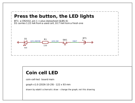
edakit schematic draw draws the schematic from graph and parts alone, without an EDA program. The note in the block
quotes the simulation – {sim:min SIM.state used/* D1 LED on} in hardware/schematic.toml – and changes when R1 or D1
change (DOCS.quote, 6.6):
What the layout must know goes into the graph as layout: the PCB designer works in a session of its own and gets
nothing else (roles, 14.1). Here the three parts a person touches or looks at are fixed, with two notes:
$ edakit handover
hand-over: coin-cell-led, graph 1.0 (2026-10-29), circuit 48984185a69a
  M-1 Critical parts (BT1, D1) checked a second time against the d…: open
  M-6 Regulatory review: circuit and parts against EU law for the …: open
board main – the plan keeps this (SYNC.plan: edakit pcb plan, the gate)
  fixed  BT1, SW1, D1
notes for the layout:
  - the cell (Ø 20 mm) stands 2 mm out of BT1 (16 mm wide) on both long sides: keep them free, with room to lever …
  - D1 next to SW1: the LED shows the press
17.9 Reviews
Two agents review the circuit before the layout, side by side, each in a session of its own; the session that designed does not review (roles, 14.1). Neither changes a file; each returns numbered findings with what to do.
- electrical-reviewer – M-1. It checked the holder and the LED again against the datasheets the sign-offs read (their SHA-256 matched), fetched the library footprints again, rebuilt the LED model by hand and judged the hints and the hand-over. Five notes, nothing critical:
- the holder's open point was aimed at JLCPCB's assembly preview, but BT1 is soldered by hand and never shows up there;
- R-1's margin (1.22 mA against 1 mA) rests on two assumed values – with a series resistance of 0 Ω the LED would get 0.48 mA, while the physics of a red LED says 30 Ω or more;
- R-2 had no number;
- the button's entry said 1.6 mm high where its drawing says 1.5;
- a comment in the board file was wrong.
- regulatory-reviewer – M-6. It checked circuit and parts against EU law for the purpose
private(chapter 15). Nothing of placing on the market applies, nothing transmits, and the board is electromagnetically benign. Four notes, none blocking: the graph called the board "a toy" – who uses it, with a coin cell that comes out by hand?; giving one of the five away makes it a gift, with duties of its own; the parts' RoHS and REACH statements are open – asking for them now would be gold plating; board and cell go to separate collection at the end.
Their notes went into one decision round. The holder's open point moved to the acceptance ("its ⊕ end on pad 1"); R-2 got its number, at most 1 µA from the cell, with M-1 as its evidence; the reasoning on R-1's margin went into D-2; and D-5 says who uses the board – adults at a desk, out of the reach of small children. Those changes are in the circuit hash, so both agents looked again, and M-1 found R-2's reason off by a factor of 100 (1 µA is 8.8 mAh a year, not 0.09). One more fix, one more look, then both signed.
The agent's result is the sign-off, bound to the circuit hash (hashes and sign-offs, 8.2):
{"id": "M-1", "phase": "export", "scope": "circuit", "done_by": "agent electrical-reviewer (own session)",
 "date": "2026-10-31", "note": "M-1: OK for state e34902df3e31…; requirements met: R-2. …"}
The note names R-2, and that is R-2's passing evidence in the gate (8.7). Any later change to graph, parts, simulation config or requirements changes the hash, and M-1 and M-6 no longer count.
In this example the hash changed three more times: edakit convert --write turned the files into the form of this
chapter's codes, with the same values and the same simulation; the cell's current limit came in (D-7), and the accept of
HINT.debounce left the graph – edakit no longer reports that hint without an MCU reading the button; BT1's entry got the
outline of holder and cell from its drawing (body.box, for the silkscreen check of 17.11). Each time both agents
looked again and signed for the new hash. M-1 checked the new accept's reason against the cell's data sheet, and one of
its looks found a hint that repeated what PATH.reverse had already checked (gaps closed, 13.9).
17.10 The gate offline
edakit gate runs stages P, G and E and writes the test protocol (chapter 8):
$ edakit gate
[ 0.0 min] step 1/2: P/G parts and graph
[ 0.0 min] step 2/2: E simulation

NOT RELEASED
  - M-5 signed for fab dbbe8aa2baf1… – checked by stage F (section 6)
  - stages not run: S (Schematic), L (Board), F (Manufacturing)
requirements: 1 passed, 1 open after the export (section 11 of the protocol)
| P Parts | parts database complete, graph pins = parts database, parts verified, … | 8 | 0 | 0 | 0 | 0 | passed |
| G Graph | structure, pin locks, voltage domains, inputs, drivers, decoupling, … | 36 | 0 | 0 | 3 | 0 | passed |
| E Simulation | ngspice operating points of all scenarios, stress of every part, … | 109 | 0 | 0 | 3 | 0 | passed |
In P and G every code without a finding counts once as passed – the codes the domains core and power switch on. G's
three accepted findings are PATH.reverse and the two hints, E's three the cell's current with SW1 held (D-7). R-2 passed
on its rows and on M-1's note; R-1 has passed its rows too and waits for its acceptance step after delivery.
Section 6 of the protocol already holds the lists for later: what M-2 looks at before paying – D1's cathode, from the
open point of its parts entry – and what M-4 tests on the delivered boards, the holder's orientation among them.
17.11 EasyEDA and the layout
EasyEDA cannot create a project through its API: you create coin-cell-led once by hand (File → New → Project) and
leave it open (the template, 6.1). On KiCad there is nothing to create: edakit writes the KiCad project itself, and
the same steps run on KiCad's files (chapter 18 shows them). Then the PCB designer takes the layout in a
session of its own (/edakit:pcb-round), starting from edakit handover.
The board file
You want the board round, "so that it gets more exciting" (D-6). That is a wish for the layout: it changes the board
file, not the circuit, so the circuit hash stays and M-1 and M-6 keep counting. Here the four rows of [place] are
written by hand; edakit pcb place --rest finds a spot for every part still without a row (the placement plan, 7.4).
Where BT1's designator and the board label go ([silk]), [looks] and [order] came after the layout review (step 5
below):
revision = "1"

[outline]                  # round, Ø 44 mm: a square whose corner radius is half its side
rect = [44, 44]
corner_radius = 22
arc_steps = 12             # 48 chords, 47 µm off the circle

[tooling]                  # JLCPCB Economic PCBA: two non-plated holes, diagonally opposite
holes = [[9, 36], [35, 8]]

[place]                    # the hand-over's fixed parts BT1, SW1, D1 – and R1, so that every part has its row (SYNC.plan)
BT1 = { x = 22, y = 24, rot = 0, side = "top" }    # the cell (Ø 20 mm) almost concentric; 10 mm free above it to lever it out
SW1 = { x = 28, y = 9, rot = 0, side = "top" }
D1  = { x = 19, y = 9, rot = 0, side = "top" }     # next to SW1: the LED shows the press
R1  = { x = 22, y = 5, rot = 180, side = "top" }   # R1.1 towards SW1, R1.2 towards D1's anode

[silk]
designators = "top"
place = { BT1 = { x = 22, y = 35.6, rot = 0, side = "top" } }   # above the cell: under it the cell hides it
board_label_region = [[11, 37.6], [33, 37.6], [33, 39.8], [11, 39.8]]   # centred above the designator

[looks]
visible = "top"            # the face people see: stage L holds its tracks and vias

[order]
remark = "Round board, no V-cut, no tabs. 2 tooling holes added by customer."

[[silk.texts]]             # the footprint's own ⊕ lies under the holder's body; this "+" stays visible – GEO.mark holds it to BT1.1
text = "+"
x = 40.3
y = 24
h_mm = 1.5
side = "top"
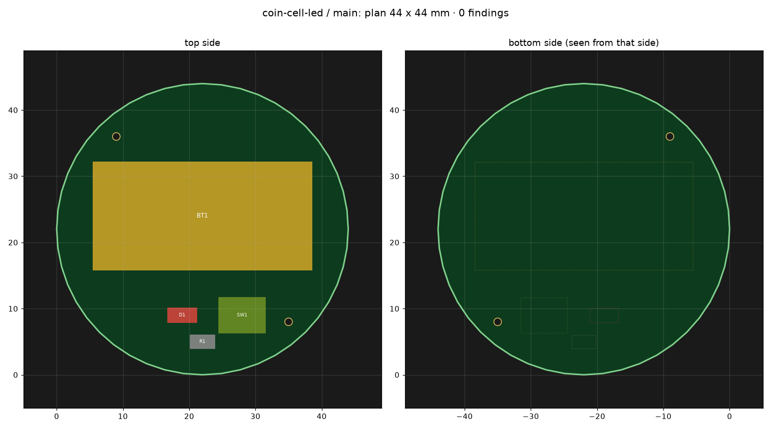
edakit pcb plan checks the plan offline, on the footprints part import cached – overlaps, outline, keep-outs, the
hand-over (SYNC.plan) – and draws it:
$ edakit pcb plan
  library geometry (edakit part import, not yet from the PCB): BT1, D1, R1, SW1
  4 fixed parts, 0 for the auto-layout; airline length of the fixed parts (without GND): 0.02 m
In EasyEDA
/edakit:start checks the bridge and claims EasyEDA for the session (parallel sessions, 11.2). Then the round runs
these commands (chapters 6 and 7), each in less than half a minute:
edakit schematic create --save,edakit schematic layout --save: the template and the readable schematic, each saved only when its netlist equals the graph:
[ 0.4 min] step 9/11: netlist against the graph
  4/4 nets match the graph
[ 0.4 min] step 10/11: ERC
  {"project_id": "current", "total_violations": 0, "error_count": 0, "warning_count": 0, "passed": true, …}
…
done: 4 placed, 0 skipped, 0 pin mismatches, 0 pin failures, 0 differing nets
edakit pcb parts --write: the four parts into the PCB, without the import dialog;edakit pcb dump: their footprints as placed, intohardware/boards/main.geometry.json;edakit pcb apply: outline, tooling holes, every part where the plan puts it:
[ 0.1 min] step 5/7: outline and holes
  outline: 48 points, 0 holes
[ 0.1 min] step 6/7: tooling holes
  2 tooling holes Ø 1.152 mm (NPTH), 0 old ones replaced
[ 0.1 min] step 7/7: pad check
  pad check (4 parts): largest deviation 0.001 mm (BT1.2)
edakit route all: Freerouting routes, the ground pours, DRC. The area outside the circle goes to Freerouting as 50 keep-out strips:
[ 0.0 min] DSN: 4 nets with >= 2 pins, 12 pads, 5 padstacks, 2 hole keep-outs, 50 edge strips, 0 keep-out pieces, …
[ 0.2 min] check: 4 nets routed, 16 track pieces, 2 vias; open: 0
[ 0.2 min] track widths (GEO.width offline): 4 nets, 0 below IPC-2221 for 1.5 x the simulated current, 0 below the …
[ 0.4 min] step 8/8: drc
[ 0.4 min]   DRC: 1 findings – {('Netlist Error', 'Import Changes', None): 1}
[ 0.5 min]   EasyEDA waits for the import acknowledgement: open Design → Import Changes once, it shows no changes …
The parts came into the PCB without EasyEDA's import, and its DRC waited until the import view had been opened
once. edakit had compared schematic and PCB beforehand and nothing differed, so that was your one click in this run
(parts without dialogs, 7.3): Design → Import Changes, it shows no changes, OK – last, after the silkscreen; then
edakit route drc reports DRC: 0 findings. Today edakit first writes the Channel ID the import sets into the
schematic parts and runs the DRC again (Import Changes, 7.5); the click is asked for only if the item stays.
4. edakit silk apply: designators where there is room, the board label, and the silkscreen checked on the Gerber
files:
  board label 'Coin cell LED rev 1' at (21.9, 38.2) mm
  top: 4 of 4 designators placed, fixed: BT1; without room: –
  top: silkscreen on mask openings 0.000 mm² (target 0), picture -> …/build/edakit/silk_main_top.png
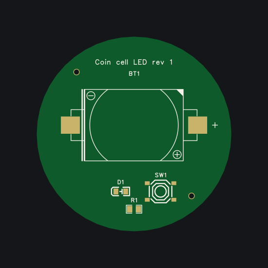
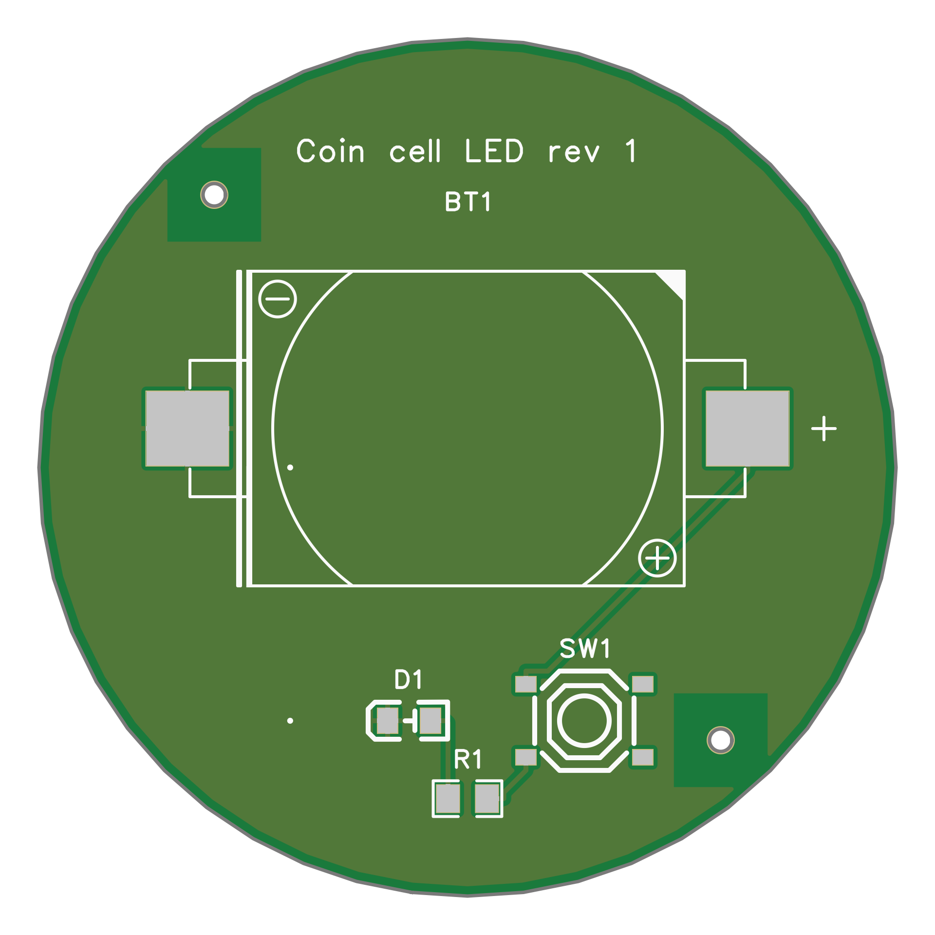
The board as the gate run draws it from the same Gerber files (pictures/board_main_top.png, 17.12) – copper,
the ground pour with its clearances, the tracks from BT1's "+" pad to SW1 and on to R1 and D1, mask and
silkscreen:
- The agent pcb-reviewer reviews the round, in a session of its own, on the manufacturing files of a gate run (17.12). Nothing blocked; it had four notes:
- BT1's designator lay under the cell – GEO.silk did not see it then; since then BT1's entry has a
body.boxfrom the holder's drawing, and GEO.silk would (grade body, 8.1); - the board label sat 8 mm left of the axis;
- without
[order]no file said that the tooling holes are the customer's – JLCPCB might drill its own on the face people see (FILES.order warns about that now, grade tooling); hand_solder_keep_mmwas not set.
You chose to move both texts above the cell, as it proposed – how the board looks is yours to decide. The designer
took the remark for JLCPCB and [looks] too. The fourth note it answered: the key covered through-hole joints only
then, and BT1 has SMD tabs, so the reviewer withdrew it. Since then it covers the SMD tabs of a part with bom:
false too, on the side the part sits on (routing, 7.5); set, it would hold BT1's tabs. A second silk apply, a
second gate run, a second look: only the top silkscreen and the order settings had changed (edakit fab diff), and
the reviewer signed M-5 for that run's files.
17.12 Release, order, acceptance
edakit gate --eda runs every stage, the last ones on the files that go to JLCPCB: the schematic equals the graph
(SYNC.schematic), the copper of the Gerber files connects what the graph connects (GEO.copper), the "+" lies next to
BT1's plus pad (GEO.mark), the BOM leaves BT1 out (SYNC.bom), the pick-and-place file has every assembled part once
(SYNC.cpl), the order settings fit JLCPCB's form (FILES.order).
The layout review M-5 is done by the agent pcb-reviewer on a run's files and bound to their fab hash; the next run with the same files counts it. Only a run whose protocol says RELEASED may be uploaded (the decision, 8.3). Here it took three runs: the first passed every stage with M-5 open, the second followed the review's notes, the third counted M-5:
$ edakit gate --eda
[ 0.0 min] step 1/4: P/G parts and graph
[ 0.0 min] step 2/4: E simulation
[ 0.0 min] step 3/4: S schematic against the graph
[ 0.0 min] step 4/4: L/F board and manufacturing files: main
RELEASED
requirements: 1 passed, 1 open after the export (section 11 of the protocol)
| S Schematic | EasyEDA schematic = graph (parts, LCSC, nets, pins, no-connects) | 1 | 0 | 0 | 0 | 0 | passed |
| L Board | PCB = graph and plan, copper from the Gerber files, DRC, footprints, track widths, holes | 34 | 0 | 0 | 0 | 0 | passed |
| F Manufacturing | BOM from the graph = EasyEDA, JLCPCB stock, pick and place, Gerber set, outline, manifest | 18 | 0 | 0 | 0 | 0 | passed |
The offline edakit gate cannot compute the fab hash without stage F: from now on it says "M-5 signed for fab
dbbe8aa2baf1… – checked by stage F" instead of naming M-5 open (hashes and sign-offs, 8.2).
The run's folder holds what goes to JLCPCB – fab/main/gerber_main.zip, bom_main.csv, cpl_main.csv, the form's
fields in order.md – and fab/polarity_main.png for M-2. A gate run is build output ([release] archive, default
"none", 8.3): a new run makes the files again from the repository, and the sign-offs say which hashes they must have.
A project publishes what is ordered as a release on GitHub, with edakit release publish; this example lives inside
edakit's repository and does not.
The order
The order goes up to JLCPCB's cart and no further – nothing in edakit orders or pays (ordering, 8.4):
edakit cart preparetakes the current release and writes the job: the upload files with their SHA-256, every field of the form from[order], the BOM JLCPCB will match. It stops unless M-6 is signed for the run's electrical hash and[cart]names the country and the shipping method; JLCPCB as the only maker needs nothing else there.- The skill cart (
/edakit:cart) fills JLCPCB's pages in your browser with Claude in Chrome, reads every field back and writes what the page showed.edakit cart checkholds that to the job and the release (ORDER.form to ORDER.finish): the fields, JLCPCB's matching of the three parts it assembles, the quote againstedakit cost, the same files. - The agent regulatory-reviewer looks at what the order adds to M-6 (15.5) – finish, quantity against the purpose,
where the maker sits –, and ORDER.review waits for its
Order: OK. - Then the skill presses the cart button and writes the order record
hardware/orders/…. Ordering and paying are yours, after M-2 in JLCPCB's assembly preview – the list in section 6 of the protocol: D1's cathode. Its "Confirm Parts Placement" puts the order into production 72 hours after it is placed unless "Do not confirm automatically" is ticked – your tick, at the form. The five holders come fromcart_lcsc.csvat LCSC; once paid,edakit cart actualputs the real prices beside the estimate and into the project's fee table.
When the boards arrive, BT1 is soldered by hand (hand_assembly.md), and M-4 works through the acceptance list of the
protocol:
- [ ] M-4 Acceptance test of every delivered board: visual check (BT1 and D1 the right way round), D1 lights while SW1
      is pressed and is dark once it is released
- [ ] C70377 CR2032-BS-6-1 (BT1): soldered by hand: the holder's ⊕ end (its chamfered corner) on pad 1, at the
      silkscreen '+'
- [ ] R-1: press SW1 with a fresh cell: D1 lights; let go: D1 is dark
Signed, it lets R-1's acceptance step pass – every requirement then has its evidence.