5 Simulation (stage E)
For you when you set up a board's scenarios or a part's behaviour model. edakit sim turns the graph into an ngspice
netlist per scenario, computes the DC operating point, and checks every part against its ratings and the circuit against
its function – in seconds, on every commit. The short way: Design the circuit.
In short. edakit sim builds an ngspice netlist from the graph and the parts entries, every IC and module a
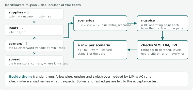
behaviour model (the netlist, 5.1). The scenarios of hardware/sim.json are supplies × loads × LED corners × the
transistors' spread, plus extra and fault scenarios, each one DC operating point (the scenarios, 5.2). Transient runs
follow a plug, an unplug or a load step; AC runs measure a frequency response, with the domain audio or guitar. The
checks hold every part to its derated limits and every input, LED and output to what the load expects (the checks, 5.3).
Routed copper adds the tracks' resistance. Switching and charge cycles are not modelled.
DC operating points come first because the expensive errors on a small board are static. A resistor that cooks at full brightness, a regulator without headroom at the low end of the USB voltage, an LED the wrong way round, a net that reaches a pin with more than it tolerates, a supply that cannot deliver the sum of all loads. A DC sweep over supply corners × load cases × LED tolerance corners finds those – and over the transistors' spread, where a stage's bias rests on it.
Where the supply itself changes – plug, unplug, a switch-over between two sources – a DC scenario sits on one side of the gap or the other; transient runs (5.2) follow the supply over time, judged by LIM.v on a net, LIM.i on a source and LIM.range for an MCU's minimum. Switching spikes and fast edges are measured on the delivered board (acceptance test): the behaviour models know no switching.
A comparison that does not hold reads as its finding is judged, as in stages P and G: fail for an error, warn for a
warning, info for a note. A new code or grade starts as a warning, which the sign-off file accepts or the gate stops
at (the decision, 8.3). A finding of the simulation is accepted as every other is, with accept and the reason on its
part or net, or on the graph keyed by "code place" (working rules, 3.4). edakit sim then prints it as accepted, its
row reads waived, and the gate lists it in section 4 of the protocol. A scenario's status follows its rows.
5.1 How the netlist is built
Parts from the graph
- Resistors, capacitors, inductors (with DCR), fuses, diodes, LEDs (model from Vf at a test current), BJTs, MOSFETs and
JFETs (kinds
njfet,pjfet:J_Q50 drain gate source) come from the graph 1:1, values and SPICE models from the parts database – a transistor's model as its entry gives it, or in a spread corner (5.2) at the end of its spread. A JFET is held to its entry in every scenario like the other transistors: |VDS| (vds_max_v), |VDG| (vdg_max_v), the gate's reverse voltage against the source (vgs_max_v), its forward gate current (ig_max_a– a gate driven above its source conducts), the drain current (id_max_a), the power. - An LED is a diode through
vf_*_vof the corner atvf_at_a, withrs_ohm(10 Ω without) and an ideality of 2 – or the one its datasheet's IV curve gives:values.vf_vs_if, points[[A, V], …]read off the curve (4.1), the slope of V − I·RS over ln I. With N = 2 the 555 blinker's red LED (Kingbright DSAO7910) lay 20–25 mV below its curve at 0.5 mA (chapter 18, M-1).edakit part lintholds the points to rising currents and volts and the ideality they give to 1 … 4. - A 0 Ω bridge (
value_ohm: 0) is itsr_max_ohm, 50 mΩ without one – ngspice finds no operating point with 0 Ω. - A capacitor with a DC-bias curve (
values.dc_bias, 4.1) is the capacitance left at the highest DC the declared ranges of its two nets put across it – a KEMET 4.7 µF 6.3 V 0603 X5R on a 0 … 5.5 V rail is 1.86 µF: the least capacitance it has in operation, the one a transient load step or an AC run around the operating point sees. The scenario's own voltage is not used, and the charge from 0 V at power-up meets more capacitance than that. Without a curve the nominal value. - A dual MOSFET in one package (FS8205A: two N-channels on a shared drain) gives its second channel the roles
gate_2andsource_2, anddrain_2when the drains are apart. The netlist builds both transistors,M_Q7andM_Q7_2, with the same model. - An RGB LED (
led_rgb) is three LEDs, one per colour with that colour'svaluesandlimits. The roles choose the layout (parts fields, 4.1): with a common cathode each colour runs fromanode_<color>tocathode, with a common anode fromanodetocathode_<color>– the layout a constant-current sink or a low-side switch per colour needs. Each colour is checked as an LED of its own (D10_RED,D10_GREEN,D10_BLUE): LIM against its ratings, SIM.state on its driver output or by the load'sleds_on, where the designator turns on all three colours andD10_REDone. - Switches, buttons, DIP switches are closed or open as the scenario's load says: a button is open unless the load
lists it in
buttons, a switch closed unless it lists it inopen–"off": {"open": ["SW1"], "leds_on": []}–, a DIP switch open unlessdip_closednames it. A changeover switch takes"throw": {"S1": "throw_b"}, defaultthrow_a; the throw moves every pole of a switch of several poles (common_2,throw_a_2… – a 3PDT footswitch's three), and REQ.value/switch judges each pole apart. - A relay is its coil (
coil_ohm) plus a contact fromcommontonowhen the load lists it inrelays_on, else tonc. That holds for every contact set: a DPDT relay's second set carries the rolescommon_2,no_2,nc_2and switches with the first, and REQ.value/switch judges each set apart. - A magnetic buzzer is its coil (
coil_ohm): its coil voltage againstv_max_v, its coil current againsti_max_a(LIM.i) – a GPIO stuck high on a 5 V buzzer of 42 Ω drives about 90 mA through it. - A potentiometer's wiper sits where the load's
potputs it –{"RV1": 0.25}, the share of its value betweenend_aandwiper, default 0.5.
Supplies
- Supplies are connectors listed under
sources(a voltage source behind a source resistance) and battery holders with a cell state (cells). A module that brings its own supply (an Arduino Nano on USB) is a source as well:plusis its 5V pin, the voltage is USB minus its on-board diode – or USB itself on a module without that diode.combine_sources(several sources, 5.2) puts it into scenarios with the other sources. - A connector that brings several rails – a Eurorack header's ±12 V – is one source with
outputsinstead ofplus: each rail its pin and itsv_ratioof the supply's voltage against the sharedminus,-1for a rail below it, e.g."J2": {"minus": "3", "outputs": {"p12": {"plus": "9", "v_ratio": 1}, "n12": {"plus": "1", "v_ratio": -1}}}with the supply"J2": 12. Each rail is a source of its own in the results (J2:p12,J2:n12), with itsr_ohm,i_max_aandi_back_max_a(the source's where the rail gives none). A current drawn from the negative rail counts as supplied, not fed back. i_min_aon a source is the least current the supply needs to stay on – USB power banks switch off below 50–100 mA after a few seconds. LIM.i checks every scenario against it, at the least current the board draws.- An MCU whose current swings – an ESP32 draws 240 mA while it transmits Wi-Fi and 20–68 mA with its radio off
(Espressif ESP32 datasheet v5.3, tables 5-4 and 4-2) – gives its upper bound as
i_core_aand its least current asi_core_min_a. The minimum load is checked in a second operating point of the scenario, with every MCU at itsi_core_min_a("current keeps the supply on (least current: U1 40 mA)"); every other check keepsi_core_a. Withouti_core_min_a,i_core_acounts for both, in one operating point. - No supply is fed backwards: where two supplies meet and nothing blocks the way, the higher one feeds the lower one –
into a PC's USB port through a module whose 5 V pin is its VBUS, into primary cells. LIM.backfeed holds the current
into every source, against its direction, to the source's
i_back_max_a, and the current into every cell of a battery holder to its cell state'si_charge_max_a–"cells": {"nimh": {"v": 1.3, "r": 0.05, "i_charge_max_a": 0.1}}for a pack its charger charges on purpose. Both arecriteria.blocking_max_a(1 mA) unless set. A cell state'si_max_aholds what a cell delivers (LIM.i/cell, a coin cell's few mA), accepted on the holder like a finding at any part –accept: {"LIM.i/cell": …}, the walkthrough's D-7.
Nets, cables and off-board loads
- Every net is one node – a track is 0 Ω – unless sim.json
coppernames it (routed copper, 5.2): then each of its pins gets a node of its own, with the routed tracks and vias as resistors in between, and every check sees the voltage at the pin. - A cable between boards (the graph's cables, 3.1) gives a net through it a node of its own on the from side
(
VIN__usb). Each wire is a resistor –r_ohm_per_wire, or the copper oflength_mand the gauge –, withl_nh_per_man inductance in series. Several wires of one net between the same two boards are resistors in parallel between the same two nodes – a pedal's ground to the DC jack, each jack's sleeve and each footswitch, wired by hand from pads. - ngspice gives each wire's current. With the cable's
i_max_a(the rating per wire of its own datasheet) every wire is held to it, derated as every current (LIM.i/cable, a warning while new). Without it, a cable that carries current gets one row of information over the scenarios – the highest current through a wire, which wire, the loss per metre of wire I² × R (highest current through a wire, no i_max_a (wire 1 – I² × R: 1.756 mW per metre of wire, AWG 26 copper at 20 °C)) – andedakit check --coveragenames it (rule checks, 3.3). The generated fault scenarios are left out of the highest current: a short is no operating current. edakit derives no rating from the gauge (rules-at-scale.md, decision 22). - Off-board loads (a servo, a motor, a strip at a connector) are the load's
external, e.g.{"J1": {"plus": "2", "minus": "1", "i_a": 0.3}}– a constant current between the two pins; it counts for the connector's contact current and for the track widths.
LED strips
An addressable LED strip (parts kind led_strip, maker-coverage FT-13) is a ladder instead of one current: its pixels
in a row between a +V rail and a GND rail of r_vdd_ohm_per_m and r_gnd_ohm_per_m, every pixel a constant current
between the two – i_idle_a, plus the load's share of full white (strips, 5.2) of the rest up to i_pixel_a. The
component gives the length, "strip": {"length_m": 5} (the graph's format, 3.1). Up to 50 pixels each is a section of
its own; a longer strip is 50 sections of equal pixel counts, each section's current at the mean place of its pixels.
The pins with the roles vdd and gnd feed the rails at the start, vdd_end and gnd_end at the far end. A cable to
the strip gives each of its pins a node of its own with the wire's resistance in between, so that every feed carries its
own current; a cable with at_m lands its wires on the rails at that place instead – an injection point. A strip on a
board of its own (wired = true, 4.5) is reached through its cables only: a pin no wire lands on is an open end of its
rail.
A strip plugged into the output of another – chained: vdd_end, gnd_end, dout of the first on nets of their own
with vdd, gnd, din of the second – is fed through the first one's rails – in the simulation, and in stage G, where
its +V rail passes a supply on (PATH.unfed) and its ground rail joins ground (PATH.ground; catalog/paths.toml).
LIM.range/strip (a warning while new) holds the supply of every pixel, measured between its two rails, to the entry's
vdd_op_min_v … vdd_op_max_v. The row names the lowest and the highest pixel ("0.0125 V (pixels 295–300, 4.95
m) … 4.823 V (pixels 1–6, 0.05 m)"), rows of information the first and the last pixel and the current of every feed. The
connector at the board's end of a wire carries that feed (LIM.i on its contacts, as for every cable). A cable's
i_max_a holds its wires, and a strip pin's own i_max_a – the rating of the strip's lead or connector – the feed at
that pin (both LIM.i/strip).
On Pololu's WS2812B strip at 60 LEDs/m (edakit/parts/Pololu_2549.json: 50 mA per pixel, 0.2 Ω/m per rail), one metre
fed at one end drops 0.59 V to its last pixel – Pololu measured 0.6 V at 3.0 A. 5 m fed at one end leave the far pixels
without supply; fed at both ends the middle sits at 1.24 V, and a third feed at 2.5 m lifts every pixel to 4.04 V or
more – through a wire that carries 7.5 A.
The model has two limits. A share below 1 is an average, while a pixel's PWM pulses draw the full current – the drop of full white is what a pulse sees. And the model's pixels keep their current down to 0.5 V, while a WS2812B draws less as its supply falls (Pololu: the far end turns redder and draws less) – the drop it gives is an upper bound.
Behaviour models
- ICs and modules are replaced by behaviour models (
values.behaviorin the parts entry):
| Model | Roles | Parameters | Behaviour |
|---|---|---|---|
ldo |
vin, vout, (gnd), (adj or fb) |
vout_v, dropout_v, iq_a; adjustable: vref_v, i_load_min_a |
output = min(vout, vin − dropout); input current = output current + iq |
buck, boost, buck_boost |
vin, vout, (fb); a boost without vout: sw, (en) |
vout_v, efficiency, iq_a; adjustable: vref_v, i_load_min_a |
ideal output – the same whether the input is above or below it; input power = output power / efficiency. An asynchronous boost whose output is no pin of its own (MT3608) has it behind the diode on its sw pin, and en low switches it off (below) |
mcu |
vsys/vin/vdd, optional vout/3v3, gpio |
v_io_v (V, or "vin" when the I/O runs from the supply pin, as on a 5 V AVR), i_core_a (default 0.03 A; an upper bound), i_core_min_a (the least current, for the minimum load only – above; default i_core_a), gpio_r_out_ohm, regulator (ldo/buck/boost/buck_boost), vout_v (regulator output, default v_io_v), efficiency, vih_v/vih_ratio, vil_v/vil_ratio |
on-board regulator feeding the core and external loads; GPIO outputs as sources with output resistance (levels from the load's gpio; null releases an output in that load – an input on its pull-up, as a key matrix's rows not scanned), pull-ups from the config; the config's inputs must sit at a defined logic level; the config's io_rail (a net or pin) is the rail of the GPIOs and pull-ups where it is not the regulator's output – a bare microcontroller (kind ic) whose on-chip regulator feeds only its core, the RP2040's 1.1 V |
cc_sink |
rext, out (or out0 … outN), vdd, oe_n |
vrext_v, iout_gain, vout_knee_v, idd_max_a |
constant-current LED driver (TLC5916, STP08CP05, …): R-EXT held at vrext, every enabled output sinks gain × I(R-EXT) with a soft knee; oe_n high = all off; pins of type output (SDO to the next driver's SDI or to an MCU input that reads the chain back) low through 50 Ω, as in logic; an unconnected SDO stays out of the netlist |
opamp |
vcc, vee (or gnd), per channel in_p, in_n, out – with a suffix for several (in_p_a, out_a, in_p_b …) |
vout_swing_v, vicm_v, iq_a, r_out_ohm, comparator |
op-amp: the output follows the inputs with an open-loop gain of 10⁴, limited to the rails plus vout_swing_v – [above vee, from vcc], e.g. [0.02, -1.5] for an output that stops 1.5 V below the supply (none: rail to rail) –, behind r_out_ohm (50 Ω); iq_a from vcc to vee; the output's own current comes from ground in the model, so a source's current misses it. LIM.range/opamp (a warning) holds every input to the common-mode range vicm_v (same form: [0, -1.5] from vee to 1.5 V below vcc) and every output to its linear range – an output at its limit while the inputs stand apart has saturated; with comparator: true the outputs are not checked – a comparator is meant to saturate |
logic |
supply pins (power_in, the role vdd or vcc first), outputs |
icc_a (a number, or {pin name: A} per supply pin), r_out_ohm (50 Ω; or [min, typ, max], taken at the spread corner – min in spread-min, max in spread-max, below), per pin state |
a sensor, transceiver, USB-UART, EEPROM or a CMOS 555: its supply current at its supply pin, a substrate diode from its ground to each supply pin (a supply driven below ground – cells upside down – is clamped by it, as on the bench), and every output in a defined state – the component's states (3.1), else the pin's state, else released for an open-drain output, released for a tri-state output unless its part ties every enable pin active (oe_n, en_n, re_n to ground, oe, en, de to a supply), low for a push-pull one. high drives the pin through r_out_ohm to its supply – the pin its ref names, else the supply pin – which then delivers what it sources; low through r_out_ohm to the part's ground; off not at all. A pull-up on a released open-drain output carries no current, one on an output held low carries V / R. Bidirectional pins rest off unless a state is given; internal pulls, an RS-485 driver and the PCF8574's current-source high are not modelled |
current |
supply pins | i_a |
constant supply current; with limits vin_min_v/vin_max_v (an own board, 4.5) LIM.range checks the voltage at its supply pins against them |
bridge |
per channel in1_x, in2_x, out1_x, out2_x, optional pwm_x and sense_x (the low sides' return, else ground); vm, en, (vcc) |
r_on_high_ohm, r_on_low_ohm (else r_out_ohm), idd_max_a, vih_v/vih_ratio, vil_v/vil_ratio |
H-bridge driver (DRV8833, TB6612) by the truth table both datasheets share: IN1 IN2 = 1 0 OUT1 high and OUT2 low, 0 1 the other way, 1 1 brake (both low), 0 0 coast (both off); PWM low brakes a driven channel, en low (nSLEEP, STBY) turns every output off. A high side is 1/r_on_high_ohm to vm, a low side 1/r_on_low_ohm to its return, each behind an ammeter: LIM.i holds each output to i_out_max_a, LIM.t the dissipation I² × r_on plus idd_max_a with rth_ja_k_per_w. No body or regenerative diodes, no undervoltage lockout, no current limit |
charger |
vin, bat, prog, (gnd, stat) |
prog_v (I = prog_v / R_PROG), vout_v (float voltage), i_pre_ratio and v_pre_v (precondition), i_term_ratio, r_on_ohm, v_headroom_v, uvlo_v, iq_a, r_out_ohm |
linear Li-ion charger (TP4056, MCP73831): constant current prog_v over the resistors from PROG to ground – and those behind a switch or solder jumper the scenario closes –, i_pre_ratio of it while the battery is below v_pre_v, constant voltage at vout_v (the current falls to 0 as the battery reaches it); no more than (vin − bat − v_headroom_v) / r_on_ohm; nothing below uvlo_v at vin or without a PROG resistor. LIM.i/charge reports the current against i_out_max_a, LIM.t the dissipation (vin − bat) × I + vin × iq_a. Termination (i_term_ratio) belongs to the charge cycle, not to an operating point: the current stays on. The status output STAT (role stat, tri-state) is low through r_out_ohm (50 Ω) while the current is above i_term_ratio of the set current (10 % without it) and high to vin below it – a full cell lights the "complete" LED –, released below uvlo_v and without a PROG resistor. CE and TEMP stay out |
protection |
vdd (the cell through its resistor), gnd (the cell's minus), od, oc, vm |
v_ovp_v, v_uvp_v, v_ocp_v (and the release voltages v_ovp_release_v, v_uvp_release_v, v_scp_v, for the record), r_out_ohm, iq_a |
one-cell protection IC (DW01A): OD at vdd while the cell is above v_uvp_v and VM − gnd below v_ocp_v, else at gnd; OC at vdd while the cell is below v_ovp_v, else at VM; above v_ovp_v OD stays high (the cell discharges through the charge MOSFET's body diode). An operating point has no history: no hysteresis, no delays – the state of a cell coming from the normal range. Within a few 10 mV of a threshold the operating point may not converge |
pd_sink |
vdd, gnd, cfg1 … cfg3, vbus_sense |
vdd_shunt_v, i_shunt_max_a, pd_request_v |
a USB PD sink (CH224K): VDD a shunt regulator at vdd_shunt_v that sinks up to i_shunt_max_a from the series resistor the board feeds it through – at the limit VDD rises with the supply (LIM.i "VDD shunt current", LIM.declared on the VDD net); the voltage the CFG levels request (pd_request_v: {"1xx": 5, "000": 9, …}, CFG1 CFG2 CFG3, x for either) is REQ.value/pd_request's, stage G – the charger is the project's source at the voltage it delivers |
pass_gate |
vref1, en, per channel a1/b1, a2/b2 … |
r_on_ohm, vgs_th_v |
a pass-gate translator (PCA9306 class): each channel a switch of r_on_ohm between its sides that conducts while the lower side sits below vref1 and en is above it – a side pulled low passes the low, released sides stay at their own pull-ups |
cc_led_driver |
vin, sense, sw, gnd, (dim) |
vsense_v ([min, typ, max]), r_on_ohm, duty_max_ratio, ripple_ratio, uvlo_v, iq_a; limits i_out_max_a, r_sense_min_ohm |
constant-current step-down LED driver with high-side sense (PT4115, AL8860): R_S from vin to sense sets I = vsense_v / R_S, the LED string from sense through the inductor to sw carries it, a Schottky diode returns from sw to vin – below |
none |
– | – | nothing |
An adjustable regulator – vref_v and a pin with the role adj (the reference between the output and ADJ: LM317,
AMS1117) or fb (the reference from FB to ground: most bucks and boosts) – takes its output from its divider instead of
vout_v. With R1 from the output to the pin and R2 from the pin to ground, VOUT = VREF × (1 + R2/R1) with adj and
VREF × (1 + R1/R2) with fb, the adjust pin's current left out as the datasheets do.
The check holds the divider to the output net's declared range (REQ.value/feedback, REQ.missing/feedback without one).
With i_load_min_a every scenario must load the regulator at least that much (LIM.range/min_load – the AMS1117 needs
10 mA, which its divider can draw itself).
An asynchronous boost converter with an external rectifier (the MT3608) has no output pin: its output is the net behind
the one diode on its sw pin, the divider's R1 runs from there. With its enable (en) low – at the pin's VIL and
below – the converter stops: its output source lets go and it draws nothing, but the graph's inductor and diode still
join the input to the output, so the output sits at VIN − VD at the load's current (TI SLVA191A: "The input voltage … is
connected to the output voltage when the device is disabled").
The protocol shows that level as information ("output with EN low"), not as a regulator off its set voltage. What hangs
on the output is judged at it: an expect of the load on the output net ({"BOOST_OUT": {"max_v": 0.5}}) fails, an LED
meant to be dark lights. HINT.boost_enable names the pattern in the check. A boost with its own vout pin – a module, a
synchronous part with its body diode – keeps its output at vout_v whatever its enable does: what passes through such a
part switched off is not in its entry.
Constant-current LED drivers
A constant-current LED buck (cc_led_driver: the PT4115, the AL8860) regulates the mean voltage across its sense
resistor: R_S – the resistors from the vin net to the sense net, in parallel – sets I = vsense_v / R_S. The model
runs at the top of vsense_v, the upper bound every check uses (the PT4115's A type 95 / 98 / 101 mV: 0.13 Ω gives
731 … 777 mA).
Its switch pulls that current into sw as long as it can – at most (V(sw) − (1 − duty_max_ratio) × V(vin)) /
(duty_max_ratio × r_on_ohm), the switch on for its maximum duty cycle. Of it the share D = 1 − V(sw) / V(vin) goes
to ground and the rest back to vin, the freewheeling diode's: the input current of an ideal buck, the switch's and the
diode's losses left out.
dim scales the current – off at the pin's VIL and below, full at VIH and above, linear in between (the datasheets' DC
dimming differs in detail). A pin's own pull-up to an internal supply (pull, pull_ohm, pull_v: the PT4115's 200 kΩ
to 5 V) is in the operating point; a dim pin without one that only capacitors touch floats, which both datasheets call
on. Below uvlo_v it is off. The LED string – LEDs anode to cathode and inductors from the sense net to the sw
net – is judged here, not by its leds_on: each LED at 80 % of its share of the set current or more, dark while dim is
low (SIM.state/cc). The checks, all warnings so far:
- LIM.i/cc: the set current,
vsense_v(max) / R_S, within the driver'si_out_max_a(the PT4115's 1.2 A, the AL8860's 1 A in TSOT25); the peak current in the string's inductor, the set current × (1 +ripple_ratio/ 2) (the PT4115 sets the ripple to 0.3 × I, the AL8860 to 0.4 × I), within itsi_sat_a - REQ.value/cc: R_S at least
r_sense_min_ohm(the PT4115's 0.082 Ω) - LIM.range/cc: the input at least what the string needs – the voltage across R_S, the LEDs and the inductor over
duty_max_ratio(the AL8860's 98 %; 1 where the datasheet gives none), plus the set current throughr_on_ohm: the on-time equation both datasheets give, TON = L × ΔI / (VIN − VLED − I × (RS + RL + RSW)). Three white LEDs on 10 V fail it.
The LEDs' own if_max_a and the inductor's i_max_a hold the simulated current (LIM.i, checks 5.3). Not in the model:
the switching itself (ripple, frequency), the switch's and the diode's losses and the driver's temperature, the
inductance range the PT4115's table recommends per current.
Other models and model rules
Two parts that are no IC have models of their own. An optocoupler with behavior: "photomos" (a PhotoMOS, AQY212)
switches between its roles load_a and load_b a resistance both ways: r_on_ohm (its maximum) while its LED carries
if_on_a or more, the leakage i_leak_a at v_load_max_v below if_off_a, linear in between. LIM.range/photomos (a
warning) holds the LED current to one side or the other, and LIM.i, LIM.v the load current and voltage to
i_load_max_a, v_load_max_v.
An ESD array (kind esd_array, USBLC6-2) has steering diodes from each protected line (io1, io2 …) to its rail
(vbus) and from ground, from vf_v at vf_at_a, and a transil from the rail to ground breaking down at vbr_min_v:
in normal operation they carry nothing.
Two model rules hold for every scenario and matter in transient runs. A regulator whose ratings give vin_min_v – an
ldo, buck, boost or buck_boost, and the mcu model's on-board regulator with vin_min_v or vsys_min_v –
locks out below it: its output and its input current fall to 0 over the 0.2 V below vin_min_v. A constant-current
load – i_core_a, idd_max_a, icc_a, i_a, an external load – falls to 0 below 0.5 V across it, so a rail nothing
feeds stays at 0 V instead of being pulled below ground. Above these voltages both are what the table says; a DC result
with every input above its minimum is the same as without them.
What a part does over time has no state model (rules-at-scale.md, decision 17): a charger's end of charge and its
recharge, a cell protection's release voltages and delays, a USB PD sink's negotiation with PG and the CC lines. Where
such a part is used a hint names the risk – HINT.charge_termination and HINT.protection_timing (domain power),
HINT.pd_negotiation (domain usb), HINT.power_path for a load on the charging cell –, and edakit check --coverage lists
the part as not simulated (SIM.state, 3.3).
Your own models
A project adds its own models in a plugin file (sim_plugin = "hardware/sim_plugin.py" in [project]; among the
project's scripts it is the kind sim, 8.6):
def my_boost(nl, des, part):            # nl: the netlist builder, see edakit/sim/netlist.py
    roles = nl.roles(des)               # role -> net
    nl._regulator(des, nl.n(roles["in"]), nl.n(roles["out"]), "0", "boost", part["values"])

MODELS = {"my_boost": my_boost}

def checks(design, cfg, res, meta, load, add):   # extra checks per scenario, SIM.state unless add names a code
    v = res.get("n_v_led", 0)
    add("SIM.state", "V_LED", "LED rail", v, "5.0 V ± 3 %", abs(v - 5.0) <= 0.15, unit=" V")
5.2 Scenarios
A board's scenarios are in hardware/sim.json. The snippet is from the
test project; the
Christmas bell's is one for a
USB-powered module with a servo:
{
  "ambient_c": 40,
  "sources": {"J1": {"plus": "1", "minus": "2", "r_ohm": 0.3, "i_max_a": 0.5}},
  "supplies": {"usb-min": {"J1": 4.75}, "usb-nom": {"J1": 5.0}, "usb-max": {"J1": 5.25}},
  "loads": {
    "idle":   {"gpio": {"LED_OE": 1}, "leds_on": []},
    "all_on": {"gpio": {"LED_OE": 0}, "cc_on": {"U2": "all"}, "buttons": ["SW1"]}
  },
  "corners": ["min", "max"],
  "mcu": {"U1": {"outputs": ["LED_SDI", "LED_CLK", "LED_LE", "LED_OE"], "pullups": ["BTN"], "pullup_ohm": 50000}},
  "derating": {"p": 0.5, "i": 0.8, "v_cap": 0.67, "v_diode": 0.67, "v_bjt": 0.67},
  "criteria": {"net_range_tol_v": 0.05, "led_on_min_ratio": 0.8, "led_off_max_a": 1e-5, "rail_tol": 0.03, "tj_max_c": 110},
  "report": ["+5V", "3V3"]
}
Scenarios = supplies × loads × corners (LED forward voltage at min/max) × spread (the transistors' corners, below), plus
extra_scenarios (e.g. "programming cable plugged in, external supply off"; "info": true turns failures into
information).
The spread of the transistors
The bias of a discrete stage – a booster, a fuzz, a phaser, a MOSFET driven from a 3.3 V output – rests on parameters
that spread from part to part more than any resistor (maker-coverage FT-17). "spread": ["min", "max"] runs every
scenario of the matrix once per corner, each transistor whose entry gives a spread at that end of it (parts fields,
4.1), named usb-nom/idle/vf-min/spread-min. typ is the model as the entry gives it; without the key every scenario
is typ, and its name has no spread part. What a corner sets, per kind (edakit/sim/spread.py):
| kind | from the entry | in the corner |
|---|---|---|
npn, pnp |
hfe_min, hfe_max; icbo_a |
BF = hFE of the corner; in max also the collector-base leakage at ambient_c as a current from the collector into the base |
nmos, pmos |
vgs_th_v [min, typ, max] |
VTO at the smaller (min) or larger (max) magnitude; KP so that RDS(on) at the lowest gate voltage of rds_on_max_ohm stays what the entry's model gives – the datasheet's maximum holds for every part |
njfet, pjfet |
idss_a, vgs_off_v [min, typ, max] |
VTO = −|VGS(off)| and BETA = IDSS / VTO² at the same end: the least IDSS with the smallest |VGS(off)| |
ic of behaviour logic |
r_out_ohm [min, typ, max] |
the output resistance at the low (min) or high (max) end: the LMC555's discharge pin, 150 Ω at 1.5 V and about 15 Ω at 5 V – one number hid the 555 blinker's current from fresh cells (chapter 18) |
min puts every parameter at the low end of its magnitude, max at the high end, all transistors of the board at the
same end – as all LEDs share a corner: the parts of one batch, and the extremes of a stage whose bias moves one way with
each transistor. A JFET's two ranges are the ends of one spread: the MMBFJ201's crossed ends (0.2 mA with −1.5 V, 1.0 mA
with −0.3 V) would need a BETA of 0.09 and 11 mA/V², a decade from the typical device's 0.98 mA/V² (its Fig. 1); the
paired ones stay within a factor of 2.3 (0.44 and 2.2 mA/V²).
A BJT's leakage follows the points of icbo_a ({"25": 5e-8, "125": 1.57e-5}, A by °C – the 2N3904's), log-linear
between them and along the nearest two beyond. It counts in max only, with the highest hFE, where both raise the
collector current. Where two transistors pull a stage in opposite directions – the Fuzz Face's Q1 and Q2 – an extra
scenario sets each part's corner itself, every other part typ:
"extra_scenarios": [{"name": "Q1 low, Q2 high", "supply": {"J1": 9}, "load": "idle",
                     "spread": {"Q1": "min", "Q2": "max"}}]
A transient run takes spread the same way (a corner, or a map per transistor). Every check runs in each corner: the
parts' limits (LIM), the states, and a load's expect on a net – the window a stage's bias must stay in. An AC run that
names no scenario of its own runs once per spread corner, around the first DC scenario of each, as <run> spread-min
and <run> spread-max: the gain moves with the bias. A transistor whose entry has no spread of its kind keeps its model
in every corner, and one row of information (SIM.config, item spread) names it.
On the example's +5V (4.75 … 5.25 V at J1), an MMBFJ201 booster with 6.8 kΩ at the drain, 1 kΩ at the source and its
gate on 1 MΩ to ground has its drain at 2.7 … 3.2 V as the typical part, 3.8 … 4.3 V in min and 1.3 … 1.8 V in max.
A window of 1.2 … 3.6 V fails in min only, and the AC gain falls below 5 dB in max at the lowest supply, where the
JFET leaves its saturation region.
The same JFET with its gate on a 1 V divider and 10 kΩ at the source holds 2.7 … 3.9 V. A 2N3904 whose base current comes through 1 MΩ from +5V has its collector at 3.9 … 4.3 V at hFE 70 against 1.9 … 2.1 V at 300 – a divider with an emitter resistor holds it.
Several sources
A board with several sources – a supply connector and a module that brings its own USB, USB and cells – gets the
combinations from combine_sources instead of by hand: a map from each source to its range, [low, high] in volts for
a source of sources, two cell states of cells for a battery holder.
"combine_sources": {"J1": [4.75, 5.25], "U1": [4.75, 5.25], "BT1": ["empty", "fresh"]}
It generates supplies named after what they set: each source alone at both ends (J1 4.75, J1 5.25, …, BT1 fresh)
and, with more than one, all of them together, each one high in turn and the others low
(J1 5.25 + U1 4.75 + BT1 empty, U1 5.25 + J1 4.75 + BT1 empty, BT1 fresh + J1 4.75 + U1 4.75) – where one supply
feeds the others hardest (LIM.backfeed: no supply fed backwards). They run with every load and corner like a supply of
supplies; edakit sim prints them once.
A hand-written case is not run twice: a supply of supplies with the same settings runs under its own name instead, and
an extra scenario with the same supply and load takes that load's case out of the matrix – the way to keep a combination
a procedure excludes ("unplug J1 while flashing") as "info": true. Without the key nothing is generated.
Fault cases
A load with "matrix": false runs only where an extra scenario names it – fault cases such as a stalled servo, whose
result you want to see and record as a decision, but which must not block every commit. Fault cases edakit can make
itself come from fault_scenarios (maker-coverage FT-8), opt-in:
"fault_scenarios": {"reversed": true, "shorted": true, "off": true, "supply": "usb-nom", "load": "idle"}
reversed: every source ofsourcesthe graph marks"source": "reversible", at its voltage reversed – beyond PATH.reverse's topology, what a shunt diode or a swapped ribbon really does;shorted: every signal wire of a cable shorted to ground at its far end (0.01 Ω at the far connector's pin);off: every source of a supply with several left out while the others stay on – an input above its own unpowered supply (LIM.v/inject).
They run on the first supply and the first load unless supply and load name others, as scenarios named
fault J1 reversed/idle, fault REMOTE shorted at J20/idle, fault BT20 off/idle. Only the parts' limits are judged
there (LIM.v, LIM.i, LIM.p, LIM.t, LIM.backfeed): a board without its supply reaches none of the states its load
expects, and its nets leave their declared ranges by design of the fault – those rows are information. A finding is a
warning at most, and the scenario's status warn: what a fault does is a question for the designer, not a release
blocker by itself.
Ambient, cells and touch
ambient_c is the ambient of the scenarios (LIM derates the fuses' hold current to it); ambient_min_c, optional, the
lowest one – LIM.i holds a fuse's hold current there against the connectors it protects (without it: the datasheet's
i_hold_a). Battery projects add "cells": {"fresh": {"v": 1.6, "r": 0.15}, "empty": {"v": 1.0, "r": 0.4}} and
supplies like {"BT1": "fresh"}. A cell state is what stands between the holder's plus and minus: two cells in
series are one state with their sum, a 9 V block on a snap one state with its voltage and internal resistance – fresh
and at its end voltage, each from the cell's datasheet in its note.
A board people reach – picked up, held, pressed – gets its touch limit: "touch_c": {"main": 48}, a map from each such
board to the temperature in °C its parts may reach (LIM.t, heat and touch 5.3). The number comes from the standard the
product follows, for the surface and the time a hand stays on it: IEC 62368-1 TS1 allows 48 °C for longer than a minute,
60 °C on plastic (51 °C on metal) for 10 s to 1 min and 77 °C (60 °C) for 1–10 s. The plain number applies at the
scenarios' ambient_c.
A limit stated for another room temperature names it: "touch_c": {"main": {"max_c": 60, "ambient_c": 25}} – a project
that designs at 40 °C for margin and requires "below 60 °C at 25 °C room" for what a hand touches. The touch item then
takes the same P × Rth(j-a) on 25 °C ("temperature where people touch at 25 °C room (board main)"); the junction items
stay at ambient_c. A board without touch_c gets no touch item; a name that is no board of edakit.toml, or another
key than max_c and ambient_c, stops the run.
Routed copper
Once a board is routed, copper brings the resistance of its tracks into every scenario:
"copper": {"nets": ["+5V", "VIN"], "oz": 1, "via_ohm": 0.001}
For each listed net and each board, edakit sim reads the routing as edakit route check does
(<artifacts>/route/<board>.ses with <board>_board.json). Every track piece becomes a resistor ρ × L / (w × t)
(0.0172 Ω·mm²/m, t = oz × 35 µm, default 1 oz), every via via_ohm (default 1 mΩ) between its layers. A pin's pads
join where a track or a via ends on them; on a layer where the board file pours the net ([[pours]]) its copper counts
as ideal.
Each pin gets its own node, and every check reads its pin: the MCU's supply, a regulator's input, a driver's headroom,
an operating range. A net's range v holds for its lowest and highest pin ("4.365 V (D9.1) … 4.442 V (D1.1)"), the
report shows the lowest. The ground net stays the reference and cannot be listed. A listed net that cannot be
annotated stays one node, and SIM.copper notes why: the board has no routing yet, a pin has no pad in the board json, or
a pin is not connected by the routed tracks, vias or pours (edakit route check).
On the example, a +5V track of 200 mm × 0.15 mm (0.655 Ω) from D1 to the loads drops the far LED anode from 4.442 V to
4.365 V; a range v: [4.45, 5.5] passes without copper and fails with it. The routing is an artifact of
edakit route, so run edakit sim again after every routing run; the gate does that in stage E. Without copper,
every net is one node.
Transient runs
transients names runs over time, each with its supplies as curves, a load and limits:
"transients": {
  "usb-unplug": {"supply": {"J1": [[0, 4.75], [0.001, 4.75], [0.00101, 0]]}, "load": "all_on", "corner": "max",
                 "stop_s": 0.0013, "step_s": 1e-6, "expect": {"+5V": {"min_v": 1.8}}},
  "usb-plug":   {"supply": {"J1": [[0, 0], [0.001, 4.75]]}, "load": "all_on", "stop_s": 0.002,
                 "expect": {"J1": {"i_max_a": 0.5}}},
  "wifi-burst": {"supply": {"J1": 4.75}, "load": "idle", "stop_s": 0.004, "step_s": 1e-5,
                 "steps": {"U1": [[0, 0.03], [0.001, 0.03], [0.00101, 0.35], [0.003, 0.35], [0.00301, 0.03]]}}
}
supply gives each source of sources a voltage or [t, V] points (seconds, rising from 0; linear in between, the
last value held) and each battery holder a cell state of cells; what it leaves out is not plugged in. load and
corner (default typ) are those of the scenarios; stop_s is the length of the run, step_s the largest time step
(default stop_s / 1000). ngspice starts from the operating point with every source at its first point – 0 V on every
net for a plug-in, the DC state for an unplug – and runs .tran.
expect holds limits per net (min_v, max_v, the lowest and highest voltage during the run) and per source
(i_max_a, the peak current it delivers): LIM.v on a net, LIM.i on a source. Every MCU whose ratings give vin_min_v
(or vsys_min_v) is held to it as well (LIM.range), from the moment its supply pin first reaches it: a plug run passes
once the MCU has started and never browns out, an unplug fails as soon as the rail falls below it.
steps lets loads change during the run, as [t, A] points (seconds rising from 0, amperes ≥ 0; linear in between, the
first value held before the first point and the last after the last): an external load of the run's load (a servo
starting or stalling, a motor's start current), an MCU's core current (a Wi-Fi burst, a radio pulse), a part of
behaviour current. Without steps they are the constants of the operating points. A load step is how the brown-out
"it resets when the motor starts" shows: the source resistance and the wires take the rail down, and the MCU's minimum
(LIM.range) fails while the step lasts.
"info": true turns failures into information. Each run gets its row in the scenario table with the lowest and highest
voltage of the report nets and the peak current of each source; a run adds no stress items and no net currents. On the
example, J1 dropping to 0 V in 10 µs leaves +5V at 2.99 V after 0.3 ms with C2 = 22 µF and at 1.59 V with 1 µF, where
the Pico 2 locks out; the plug-in takes 0.22 A from J1 while C2 charges.
A switch-over between two sources – two P-MOSFETs back to back next to a USB diode – is a run with both in supply, the
one ramping while the other holds. Its gap comes from the MOSFETs' thresholds and body diodes, and the capacitors bridge
it or not. Without transients nothing runs.
AC runs
ac names small-signal runs around an operating point – only where it names an expectation, and only with the domain
audio or guitar on (decision 9 of rules-at-scale.md; without either, a note SIM.config/off says that nothing ran):
"ac": {
  "output_coupling": {"about": "C22 / R24: f = 1 / (2π · 100 kΩ · 1 µF) = 1.6 Hz",
                      "input": "GTR_IN", "output": "BUF_OUT", "scenario": "usb-nom/idle/vf-min", "source_ohm": 0,
                      "expect": {"gain_db": [{"at_hz": 1000, "min": -0.5, "max": 0.5}], "low_hz": {"max": 10},
                                 "high_hz": {"min": 10000}},
                      "from_hz": 1, "to_hz": 100000, "points": 20}
}
input is the net driven with 1 V AC – through 1 F, so its DC stays the operating point's – behind source_ohm, the
source's own resistance (default none), or behind source, a source model of the audio band (maker-coverage FT-18,
decision 20 of rules-at-scale.md), one of three:
source |
Model | Values |
|---|---|---|
{"pickup": ROW, "l_h": 2.5} or {"r_ohm", "l_h", "c_f"} |
a magnetic pickup: R and L in series, C across its output | coil resistance, inductance, winding capacitance |
{"piezo": ROW} or {"c_series_f"} |
a piezo disc: 1 V behind its capacitance | the disc's capacitance |
{"microphone": ROW} or {"rl_ohm"} |
an electret capsule: its FET a current source of 1 V / RL into the input net, no DC | the load resistor of the data sheet's measurement circuit |
ROW is a row of edakit/catalog/tables/audio_sources.toml – pickups of Seymour Duncan, DiMarzio and Mojotone, Murata's
7BB piezo discs, electret capsules of CUI and INGHAi –, each with what its maker states and the page or data sheet it
was read from (the catalog page lists them). A value the row states is not given again – a project that measured its own
pickup gives its numbers instead of the row –, one the row lacks is the project's.
The makers reachable state a pickup's DC resistance, Seymour Duncan also its resonant peak, none its inductance or
capacitance: a named pickup needs l_h from the project, measured or published, with its source in note; without it
the run stops with the reason. edakit derives no inductance from a resonant peak whose load the maker does not state.
c_f holds the winding's capacitance and whatever the project lumps with it; a cable of the graph brings its own
(below).
A piezo's corner with the input's resistance is 1 / (2π · R · C): Murata's 7BB-20-6L0, 10 nF, into 1 MΩ gives 16 Hz,
into 100 kΩ 159 Hz; the low end of its ±30 % a project checks with c_series_f (7 nF) in place of the row.
A microphone's 0 dB is the capsule's output into its data sheet's RL alone: its RL is a resistor of the graph, from the input net to a supply (a run whose input has no resistor chain to a fixed level stops – the capsule's FET would have no bias). An RL larger than the data sheet's gives more, a smaller less; sensitivity, operating voltage and current are in the row for the reader, the model does not use them.
A cable of the graph with c_pf_per_m and length_m (the graph's format, 3.1) puts c_pf_per_m × length_m from each of
its wires to its wire on ground, at its from end – in AC runs only, a cable without a wire on ground adds none. An
instrument cable from a guitar board to the pedal's jack lowers the pickup's resonance by √(C / (C + C_cable)): 3 m of
100 pF/m on 500 pF moves 4.5 kHz to 3.6 kHz.
output is the net measured against its board's ground; scenario the DC scenario linearised around (default the
first – with spread, the first of each corner). ngspice runs .ac dec from from_hz to to_hz with points per
decade (default: a decade beyond the expectation's frequencies on each side, 20 per decade). The gain is 20·log10
|V(output) / V(source)| – with a source resistance it includes what the input's load does to the source –; a corner is
where the gain falls 3.01 dB below its largest value in the sweep, interpolated in log f, and a corner outside the sweep
is reported as beyond it (below the sweep it meets a max the sweep reaches, never a min).
Each expectation is a row, a missed one SIM.response (grade gain or corner), a warning while new; the run gets its row
in the scenario table and its curve in result.json (ac, with the source model it ran: kind, row and values).
"info": true makes the run's rows information, as a transient run's: a missed expectation is a row marked info and no
finding – the response a project computes from its schematic where no source states what the design intends (the
GuitarML pedals of tests/open_designs/: the TS's mid hump from 1/(2π·4.7 kΩ·47 nF), the boost's gain from R3/R4). The
op-amp model has no gain-bandwidth: an upper corner comes from the passive parts only.
On the reference circuits, the guitar buffer's output coupling C22 / R24 gives 1.59 Hz, with 100 nF instead of 1 µF 15.9
Hz – SIM.response; the audio input's R20 / C21 low-pass 15.9 kHz, with 100 nF 1.6 kHz. With a pickup
(tests/test_audio_sources.py: Seymour Duncan's SH-1 neck, 7.43 kΩ, and 2.5 H and 500 pF chosen for the test) into a
500 kΩ volume pot and a 1 MΩ input the resonance at 4.5 kHz rises 9.9 dB, into 250 kΩ 6.7 dB – the simulation agrees
with the coil's formula within 0.1 dB.
What a load expects
expect in a load holds what the project expects there, as in a transient run: per source i_max_a, i_min_a – a
sleep current budget, the evidence for a battery-life requirement (LIM.i) –, per battery holder the same for the current
its cells deliver in that load ("off means off": {"BT1": {"i_max_a": 1e-6}}, the KiCad walkthrough, chapter 18), per
net min_v, max_v (LIM.v).
strips gives each LED strip of a load the share of full white its pixels show – {"DS1": 1} every pixel at full
white, 0.25 a quarter of it on average; a strip the load does not list is dark (its i_idle_a). A name that is no LED
strip, or a share outside 0 … 1, is SIM.config.
leds_on lists the LEDs that light in a load – the designator, or D10_RED for one colour of an RGB LED, "all" for
every one; the others are expected dark. LEDs on the output of a constant-current sink go by the channel instead (LEDs
on a sink, 5.3). As soon as an LED is on no driver output, every load needs leds_on, [] when none lights
(SIM.driver).
5.3 Checks
The simulation is a producer: it computes the voltages, currents, powers and temperatures of every scenario, and the engines judge them as they judge the declared ranges of the graph – LIM against the limits of the parts entries (derated, chapter 14.2), LVL against the thresholds. Their codes are in the rule checks (3.3), with what stage E adds. Every row of the protocol carries its code, the scenario and the item. The codes of the simulation itself, generated from the catalog:
| Code | Title | Severity |
|---|---|---|
SIM.config |
simulation config readable | error, off: note; replaces E-1, E-3 |
SIM.converge |
every scenario converges | error; replaces E-1 |
SIM.state |
the circuit does what the scenario expects | error, cc: warning; replaces E-3 |
SIM.driver |
every LED has a known driver | error; replaces E-4 |
SIM.response |
frequency response as expected | warning, gain: warning, corner: warning |
SIM.copper |
copper annotated | note; replaces E-1 |
Rule, why, fix and sources of each: edakit explain CODE, or the code on its page of the catalog.
Power, heat and touch
Power. What a part dissipates at the operating point of every scenario is held to the p_max_w of its entry,
derated by derating.p of sim.json (50 % by default, catalog/tables/derating.toml): a resistor's I²R, a transistor's
VCE × IC + VBE × IB, a MOSFET's VDS × ID, a JFET's VDS × ID + VGS × IG, and an LED's VF × IF, its series resistance
included – each colour of an RGB LED against its colour's p_max_w where the entry gives its limits per colour. LIM.i
alone does not hold an LED: one below its if_max_a with a high forward voltage can be above its power rating.
The walkthrough's red LED dissipates 14.75 mW at the most, against 32.5 mW, half its 65 mW (what the checks found,
17.6). A part without p_max_w gets no LIM.p row; a diode's power counts into its junction temperature only (below).
Heat and touch. Half the power rating is no temperature: an AO3401A (125 K/W) at LIM.p's 0.45 W runs at 96 °C at 40
°C ambient. Every part whose entry gives rth_ja_k_per_w gets its junction temperature in every scenario, ambient_c +
P × Rth(j-a), with P the power of all its elements – as for LIM.p, a diode's VF × IF and a MOSFET's body diode included
(ngspice counts it in the drain current). It is held to the part's tj_max_c, at most the criteria's tj_max_c
(default 125 °C) – the limit of the LDO and LED driver items of LIM.t as well ("junction temperature at 40 °C: 0.0751 W
× 125 K/W").
An MCU module's own LDO (regulator: "ldo") gets its LIM.t item once the module's limits give rth_ja_k_per_w – the
θJA of the regulator on the module, from the regulator's datasheet, like tj_max_c there. With all the current it
carries, P = (vin − vout) × (the load at the module's 3V3 pin + its i_core_a). The model's regulator feeds the core,
so for a module whose core runs from its supply pin instead (an AVR at 5 V, v_io_v: "vin") it is an upper bound.
The LILYGO T-Display's AP2112K-3.3 (184 K/W in SOT25) feeding an ESP32 that transmits Wi-Fi turns 0.5 W into heat at 4.83 V in, 122 °C at 30 °C ambient ("junction temperature of the on-board regulator at 30 °C: 0.5 W × 184 K/W"). A buck, on a module or not, gets no item, and neither does a module whose 3V3 pin is on no net – the model has no regulator then.
On a board of touch_c the same temperature – the upper bound of the part's surface – is held to the touch limit, for
the LDOs and LED drivers too ("temperature where people touch (board main)"), on the room temperature the limit names,
where it names one (the touch limit, 5.2). A P-MOSFET switched off while fresh cells and USB meet passes every rating
with 0.27 W in its body diode and still reaches 74 °C under a hand.
Levels and LEDs
Operating range and logic levels. A part whose entry gives its operating supply range – limits vdd_op_min_v /
vdd_op_max_v for its supply pins (the power_in pins with the role vdd or vcc, else all of them), or v_op_min_v
/ v_op_max_v on a pin – is supplied inside it in every scenario, measured from the pin to the part's own ground pin.
An input pin (type input) of a part with thresholds – vih_v | vih_ratio and vil_v | vil_ratio on the pin, else
in the part's values; a ratio is taken of the voltage at the part's supply pin – sits at ≤ VIL or ≥ VIH ("input level
undefined at OE(ED2)").
A DC scenario drives most outputs low, so the high level of every MCU output on the input's net (behind 0 Ω bridges too)
is held against VIH as well, whatever the load drives: v_io_v, or the supply pin's voltage with "vin" ("output high
level reaches VIH of U2 SDI"). These are the recommended operating conditions of the datasheet, not its absolute maxima
(LIM.v): a 5 V-only LED driver behind a 3.3 V MCU stays inside every absolute maximum and does not work. A part entry
without them gets no item; an MCU's own inputs go by the config's inputs.
LEDs. A reversed LED on a driver output fails as "LED reversed"; a reversed LED elsewhere stays dark where it should
light. That is the polarity check of the graph – for an LED with an expected state. SIM.driver makes sure every LED has
one: an LED on no driver output in a load without leds_on would be skipped, and so would an LED whose parts entry the
netlist cannot read, with neither polarity nor current checked. Both fail SIM.driver instead. An LED with a pin in nc
(the unused colour of an RGB LED) is not simulated and needs nothing.
LEDs on a sink. An LED counts on the output of a constant-current sink when its cathode is on that output –
directly, behind 0 Ω bridges, or behind one resistor that joins its cathode net to this output and no other: a series
resistor that takes voltage off the driver, or several LEDs in parallel on one channel, each with its balancing
resistor. The LEDs on one output form a group, and the load's leds_on does not apply to them; the load's cc_on names
the outputs of each driver that are on – {"U2": "all"} or a list of output nets or pin names – while its oe_n is
low.
With the channel on, each LED carries at least led_on_min_ratio (default 0.8) × set current / number of LEDs in the
group ("LED current (LED7)"), and min/mean of the group reaches chain_min_ratio (default 0.7; both under criteria);
with the channel off, each is dark. A cathode net that reaches two outputs through resistors, and the ground net, count
on no output – such an LED goes by leds_on.
5.4 Track widths from the simulation
edakit sim writes the largest current of a single part per net to <artifacts>/sim/net_currents.json (the supply
current also on both supply nets, ground included). edakit pcb plan derives net classes from it (IPC-2221 outer layer,
1 oz, 10 K rise, × 1.5) with practical minimum widths from [net_classes] of the board file; the gate check GEO.width
fails a track below the IPC width and warns below the class width.
edakit route check measures the same on the routing before anything is written to EasyEDA, and with
[routing] widths = "sim" the router gets those IPC widths itself (routing with Freerouting, 7.5). GEO.width shows the
voltage drop as an upper bound, as information; the simulation computes the drop itself once the board is routed and
copper names the net (routed copper, 5.2).
5.5 Every check seen red
The tests in tests/test_sim.py build faults into copies of the example (a reversed LED, an overloaded resistor, a too
narrow voltage range, a too weak supply) and expect the matching check to fail. Do the same for checks you add in a
plugin: a check that never failed may not work. The other layers of edakit's tests: verification and validation
(19.2).