18 Walkthrough on KiCad: a 555 blinker
For you if you draw in KiCad, run a board from cells behind a power switch, or want to see an IC through every step. After it you have followed a board on KiCad from the idea to released manufacturing files. The short way: the steps.
Switch it on and a red LED blinks about once a second, from two AAA cells; switch it off and the cells deliver nothing. The chapter tells what this board adds to the coin cell board of chapter 17; who does what and why each step comes where it does stands there, for both tool chains. The project is examples/blinker-555.
What it shows that chapter 17 does not:
- KiCad end to end (KiCad as the tool chain, chapter 16): a real board through edakit's KiCad tool chain, with the
real LCSC footprints – through-hole pins, a slide switch's pegs, a SOIC-8 –, up to RELEASED and
edakit export. - An IC with a supply range, held to cells that run down.
- Cells in series, an end voltage and a power switch: "off means off" with a number, a current budget per load.
- A circuit whose function is a time. edakit evaluates each DC state of the board; the blink rate is computed in the decision log and counted on the finished board.
- The graph as TOML from the start (the graph's format, 3.1).
State 2026-10-31: the outputs are from real runs with KiCad 10.0.6, ngspice 47 and Freerouting 2.4.1, shortened where a
…stands. Every gap the run found was closed in edakit on its way (gaps closed, 13.10).
18.1 The steps at a glance
| Step | Who | New compared to chapter 17 | |
|---|---|---|---|
| 1 | Set up | /edakit:new-project |
the tool chain answered with KiCad 10: toolchain = "kicad", graph = "hardware/graph.toml" |
| 2 | What it must do | /edakit:requirements |
an end voltage per cell; "off means off" with a number; a requirement on a time whose only evidence is accept |
| 3 | Parts | part-search | an IC chosen by its supply range; a through-hole holder and switch soldered by hand |
| 4 | Circuit | /edakit:circuit-design |
the graph written as TOML; the 555 as behaviour logic, its lit phase in the component's states |
| 5 | What the checks found | Claude proposes, you decide | an LED that cannot light at the end voltage; reverse polarity at an IC; the timing as a decision |
| 6 | Stock and cost | edakit stock, cost, order |
holder and switch by hand beside an Economic order for the SMD parts |
| 7 | Drawing and hand-over | schematic draw, handover |
the holder on the bottom, the switch at the edge |
| 8 | Reviews | electrical-reviewer, regulatory-reviewer | M-1 found the lit-phase budget held only on paper (18.8) |
| 9 | The gate without a tool chain | edakit gate |
– |
| 10 | EDA project | – | nothing to do: edakit writes build/edakit/kicad/main/ |
| 11 | Layout | /edakit:pcb-round |
pcb place --rest (KiCad has no auto-layout), pcb apply, route all with kicad-cli's zone fill and DRC, silk apply |
| 12 | Release | edakit gate --eda, edakit export |
stages S, L, F on kicad-cli's netlist, ERC, DRC, Gerber, drill and position file |
| 13 | Order | – | decided at the release (18.12) |
| 14 | Acceptance | you | the blink rate counted at two voltages: the evidence the simulation does not give |
Steps 3 to 12 need ngspice, Freerouting and kicad-cli (install, 2.2; KiCad's setup, 16.2). One session did steps 1
to 12, the layout starting from edakit handover alone; the reviews ran as agents in contexts of their own.
18.2 Set up
The interview of /edakit:new-project blinker-555 main runs as in chapter 17 (set up, 17.2), with KiCad as the tool
chain. JLCPCB makes the board and assembles the SMD parts on the top side (Economic); the 2×AAA holder and the slide
switch are through-hole and soldered by hand, the holder on the bottom. Built for oneself in the EU; the answers are
D-1:
[project]
name = "blinker-555"             # the KiCad project in build/edakit/kicad/main/ – edakit writes it, nothing by hand
toolchain = "kicad"              # KiCad 10 as the tool chain (handbook 16): no EasyEDA documents to name
quantity = 5
graph = "hardware/graph.toml"    # the graph as TOML; edakit graph json --write keeps hardware/graph.json beside it
requirements = "hardware/requirements.toml"

[boards.main]
title = "555 blinker"

[release]
assembly = { sides = ["top"], smd_only = true }   # Economic PCBA: one side, SMD only (SYNC.cpl)
edakit doctor names KiCad instead of Node, server and bridge: "OK KiCad 10.0.6 (kicad-cli: /usr/bin/kicad-cli)".
The purpose is private: your own use only. If you build the board from this chapter and give it away or sell it,
that is another purpose and needs a review M-6 of its own (the regulatory review, chapter 15). That review is
support, not legal advice: it claims no correctness, and nothing in it is legally guaranteed.
18.3 What it must do
Two needs and four requirements, every number put to you in one round (hardware/requirements.toml, D-2):
| binding | text, as accepted | evidence | |
|---|---|---|---|
| R-1 | must | With SW1 on, D1 carries at least 1 mA while it is lit – from two fresh alkaline AAA cells (3.2 V) down to two used to 1.0 V each (2.0 V). | rows SIM.state * D1 LED on; accept |
| R-2 | must | With SW1 on, D1 flashes 48 to 72 times a minute – at 3.2 V and at 2.0 V. | accept: count for 60 s from a lab supply |
| R-3 | must | With SW1 off, D1 is dark and the board draws at most 1 µA from the cells. | rows |
| R-4 | should | With SW1 on and D1 lit, the board draws at most 5 mA from the cells. | rows |
The end voltage is your decision: at 1.0 V per cell an alkaline AAA has given about 90 % of its capacity. R-2 is a
time, and nothing in edakit computes a time (decision T of the concept). Its only evidence is the count at the
acceptance, so it waits until the boards are in your hand (edakit gate: "open after the export"). Two numbers did
not survive the run: R-1 changed with the checks' findings (18.6), R-4 with the reviews (18.8).
18.4 Parts
The 555 by its supply range. An NE555 needs 4.5 V; two AAA cells give 3.2 V fresh. JLCPCB's catalogue has the CMOS ones:
$ edakit part search "TLC555"
C6986      TLC555CDR        Texas Instruments       Extended     96600  SOIC-8 – 555 Timers / Counters
…
$ edakit part search "LMC555"
C90760     LMC555CMX/NOPB      Texas Instruments       Extended     18469  SOIC-8 – 555 Timers / Counters
…
The datasheets settle it: the TLC555 runs from 2 V – the end voltage exactly, the cells' internal resistance taking
the rest –, the LMC555 from 1.5 V (SNAS558M, "1.5 V supply operating voltage ensured"). U1 is the LMC555, its entry
behaviour logic (the netlist, 5.1): icc_a 250 µA, the supply range for LIM.range, THR, TRIG and CV as analog
comparator inputs, DIS an output with drive = "open_drain":
"7": {"name": "DC", "type": "output", "role": "dis", "drive": "open_drain", "v_min_v": -0.3, "v_rel_max_v": 0.3,
      "hint": "discharge: open drain, low in phase with the output (pin functions, p. 3); VDIS ≤ 150 mV at 1 mA with V+ 1.5 V, …"},
"8": {"name": "V+", "type": "power_in", "role": "vdd",
      "needs": [{"what": "capacitor", "c_min_f": 1e-07, "source": "TI SNAS558M, 10 Power Supply Recommendations: …"}]}
…
"values": {"behavior": "logic", "icc_a": 0.00025, "r_out_ohm": [15, 50, 150]},
"limits": {"vdd_max_v": 15, "vdd_op_min_v": 1.5, "vdd_op_max_v": 15, …}
r_out_ohm was one number, 150 Ω, until the review M-1 (the reviews, 18.8).
Holder and switch by hand. The holder is a Keystone 2468 – two AAA cells in series, PC pins Ø 0.79 mm, 53.0 ×
24.6 × 13 mm, 178 at LCSC (C254917); body.box gives its outline for the plan and the silkscreen check. The switch
is a horizontal SPDT slide switch, SK12D07VG4 (C393937): three terminals 2 mm apart and two frame pegs, which the
graph puts into nc. Both have a lead per pad for GEO.hole and are soldered by hand (bom = false). Their
open points go to the acceptance: which knob position closes pin 1, the holder's "+" in pad 2.
18.5 Circuit
The graph is TOML from the first line: components and nets as tables, pins by role.
[components.U1]
type = "ic"
label = "CMOS 555 timer"
part = "LMC555CMX/NOPB"
lcsc = "C90760"
states = { OUTPUT = "low", DC = "low" }
notes = "Runs from 1.5 V. The simulation holds the phase in which D1 is lit: OUTPUT low, DC (discharge) low. …"

[nets.LED_K]
pins = ["D1.cathode", "U1.dis"]
v = [0, 3.3]
edakit graph json --write writes the resolved hardware/graph.json beside it after every change.
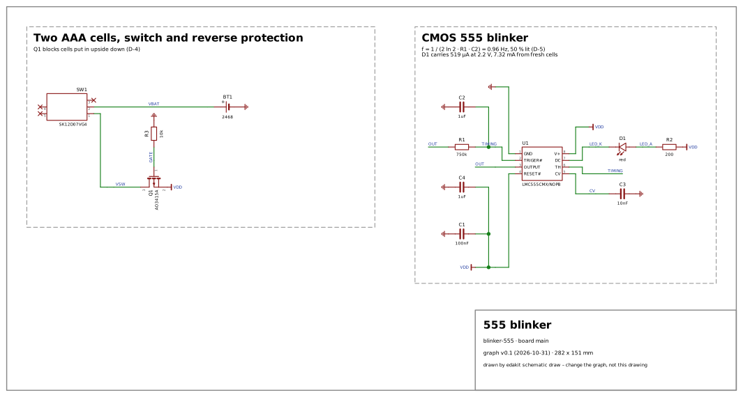
The topology is the CMOS 555's 50 % astable: R1 from OUTPUT charges and discharges C2 between 1/3 and 2/3 of VDD,
and DIS is free to sink D1 from VDD through R2. A discharge pin is the strongest output a CMOS 555 has at a low supply,
and the classic astable's current through RA in the dark phase is gone. The simulation has no time: in every scenario
states holds U1 in the phase in which D1 is lit; the dark phase is computed in the decision log (D-7).
The cells in sim.json are two states of the holder, the switch one load each:
"cells": {
  "fresh": {"v": 3.2, "r": 0.6, "note": "… 0.15–0.3 Ohm each fresh (Energizer E92 datasheet) – 0.3 Ohm each"},
  "used": {"v": 2.0, "r": 2.0, "note": "… 1 Ohm each assumed – …"}
},
"loads": {
  "on": {"about": "SW1 on, the 555 in the phase in which D1 is lit", "leds_on": ["D1"],
         "expect": {"BT1": {"i_max_a": 0.005}}},
  "off": {"about": "SW1 off", "throw": {"SW1": "throw_b"}, "leds_on": [], "expect": {"BT1": {"i_max_a": 1e-06}}}
}
expect on a battery holder is the current budget of R-3 and R-4 – the current from its cells in that load. The
first edakit check and edakit sim:
PATH.reverse – reverse polarity blocked: 3 error
  G  U1.8 on VDD: a reversed source reaches this pin without a blocking device   (catalog/paths.toml [reverse]) …
LVL.undefined – input defined while the firmware is not running: 1 warning
  G  LED_K: driven only by outputs that let go (U1.7) and nothing holds it – released, it floats
…
$ edakit sim
244 comparisons: fail 13, pass 231

LIM.range – supplied inside the operating range: 4 error
  E  [fresh/off/vf-min] U1: supply voltage at V+ inside its operating range: 2.296e-25 V, expected 1.5 … 15 V
SIM.config – simulation config readable: 8 error
  E  [fresh/on/vf-min] expect of the load: BT1 is neither a source nor a net, …
SIM.state – the circuit does what the scenario expects: 1 error
  E  [used/on/vf-max] D1: LED on: 7.779e-06 A, expected ≥ 1 mA
Three of these were edakit's: a load's expect knew no battery holder, U1 with SW1 open counted as supplied below
its range instead of switched off, and LED_K was told to take a pull-up although nothing reads it – D1 is the
discharge pin's load. All three were fixed before going on (gaps closed, 13.10); what stayed was the
circuit's.
18.6 What the checks found
The LED at the end voltage (SIM.state, D-3). At 2.0 V and its highest forward voltage (2.6 V at 20 mA) D1 gets 8 µA. No red LED reaches 1 mA there by its datasheet with a series resistor: at the end voltage it has 0.1–0.2 V of headroom, from fresh cells 1.5 V, and a resistor's current scales with it – ten times as much, where R-4 allowed five.
You chose a low-current LED and a new number for R-1: D1 is a Kingbright APTD2012LSURCK, specified at 2 mA
(VF 1.5–2.1 V, 60–150 mcd), at 0.5 mA brighter on axis than the first LED at 1 mA, in a narrower beam; R-1 asks for at
least 0.5 mA down to 1.1 V per cell, 2.2 V for the pair. sim.json follows: the cell state used at 2.2 V,
criteria.led_on_min_a 0.0005. R2 became 200 Ω – 220 Ω gave 0.498 mA.
Cells upside down (PATH.reverse, D-4). Both cells reversed put −3.2 V on U1, rated −0.3 V. On the coin cell board
the LED blocked by itself (17.6); here an IC takes it, through its substrate diode, with amps. A Schottky diode would
cost 0.15–0.25 V of the 2.2 V; a P-MOSFET costs nothing at these currents – if it is fully on at the end voltage. The
block reverse-pmos brings an AO3401A, specified from VGS −2.5 V; Q1 is an AO3415A (C133233), specified from
−1.8 V (65 mΩ), behind SW1, its gate through R3 to ground. An extra scenario holds it to its job:
"reversed": {"v": -3.2, "r": 0.6, "note": "both fresh cells put in upside down – the holder takes them that way"}
…
"extra_scenarios": [{"name": "reversed/on", "supply": {"BT1": "reversed"}, "load": "on_reversed", "corner": "max"}]
Its first run showed VDD at −0.84 V – behind a blocking Q1 the net hung on 1 pA of leakage and the simulator's
1 TΩ shunt. A CMOS IC has a diode from its ground to its supply that holds such a node. The behaviour logic has it
now (13.10), and VDD sits at −0.15 V, D1 dark, 4 pA from the cells.
The blink rate (D-5). No check, a computation: with the thresholds at 1/3 and 2/3 of VDD each half period is ln 2 · R1 · C2, independent of the supply, so T = 1.386 · R1 · C2. The spread is the work: R1 ±1 %, C2 ±10 % (X7R; its DC bias at 3.2 V on a 50 V part below 1 %), and U1's thresholds. The datasheet gives the monostable's timing accuracy at 1.5 V (0.9–1.25 ms for 1.1 ms), an upper threshold between 0.593 and 0.713 of VDD. Worst case, T lies between 0.798 and 1.204 times the nominal.
With 680 kΩ (no loading fee) that is 53 to 80 flashes a minute; you chose 750 kΩ (a loading fee of about 3 USD per order): 57.7 nominal, 47.9 to 72.3 – both edges of R-2's window touched. The count at the acceptance stays the evidence. The first period after switch-on is longer, 0.82 s dark instead of 0.52 s: C2 starts at 0 V.
The dark phase (D-7). OUTPUT high, DIS released: D1 and R2 carry nothing, R1 at most 2.8 µA, U1 at most 250 µA. Half lit and half dark, the mean is 3 to 4 mA from fresh cells – eleven to fourteen days of blinking.
The hints: HINT.bulk (no cable; C1 100 nF and C4 1 µF at U1, as its datasheet asks), HINT.lithium (alkaline cells), HINT.gate (Q1's gate never switches) and HINT.thermal_copper on U1, Q1 and D1 are accepted with their reasons (D-6). Then: 0 errors, 6 accepted.
18.7 Stock and cost
$ edakit stock
hardware/stock.json: 9 of 9 assembled parts asked, economic PCBA ([release] assembly.sides top: one side), 5 boards
  C90760      U1           LMC555CMX/NOPB, Extended Part, stock 18469 / 5 needed, MSL 1, Economic and Standard, …
  …
The first edakit cost named five Extended parts at 3.07 USD loading fee each; a Basic 10 nF in 0805 (C1710)
replaced the one at CV. With the board's size known:
board main, 60 × 28 mm: Economic PCBA ([release] assembly.sides top: one side)
  PCB                                                10.70  at most the price of the smallest size in the fee table, …
  …
  loading fee, 4 types                               12.28
  …
  board main                                         36.61 USD
what drives the cost:
  R1 C17817 Extended Part – 3.07 loading fee
  …
edakit order puts holder and switch into the LCSC cart and onto the hand-assembly list:
bom_main.csv: 9 lines for the assembler (5 boards)
cart_lcsc.csv: 2 lines, C254917 x 5, C393937 x 5
hand_assembly.md: 2 parts by hand, 0 items off the board
18.8 Drawing, hand-over, reviews
$ edakit handover
board main – the plan keeps this (SYNC.plan: edakit pcb plan, the gate)
  fixed  BT1, SW1, D1
  edge   SW1
  near   one of C1, C4 next to U1 – decoupling of VDD, a capacitor of its own (derived)
notes for the layout:
  - BT1 (Keystone 2468, 53.0 × 24.6 × 13 mm) on the bottom, the board about its size; its two PC pins are soldered on the top side
  - SW1 at the board's edge, its knob out over it; its terminals and pegs are soldered on the bottom – not under BT1's body
  …
The two reviews ran side by side.
- electrical-reviewer – M-1. Nothing blocked; one finding mattered. R-4's rows passed only because U1's discharge
pin was simulated at 150 Ω – the datasheet's maximum at 1.5 V. At 3.2 V the pin is far stronger (the typical part
at 5 V: 15 Ω), and a real board draws 6 to 8 mA while D1 is lit. A logic part's
r_out_ohmtakes a range now, [min, typ, max] at the spread corner (the netlist, 5.1), andsim.jsonruns"spread": ["min", "max"]: 7.6 mA from fresh cells. R-1 and 5 mA cannot both hold with a series resistor; you set R-4 to 8 mA (D-9). - electrical-reviewer, its notes. Eight, none blocking – among them the hand-over's note on C2, which named the wrong pin, and AAA-sized Li-ion cells (10440, 3.7 V each), which fit the holder and would overload Q1, R2 and D1: "2x AAA 1.5 V" is printed on the board now.
- regulatory-reviewer – M-6. For the purpose
private: nothing of placing on the market applies, nothing transmits, the electromagnetic requirements are met in substance (an active part, so not "inherently benign"), spent cells and the board go to separate collection.
Both looked again after D-9 and signed for the new circuit hash, M-1 with "requirements met: R-1, R-3, R-4".
18.9 The gate without a tool chain
edakit gate runs P, G and E as on the coin cell board (17.10); with the reviews signed, only M-5 and the stages S,
L, F are left. R-3 and
R-4 pass on their rows, R-1 waits for its acceptance step, R-2 has nothing else:
| P Parts | parts database complete, graph pins = parts database, parts verified, parts orderable | 8 | 0 | 0 | 0 | 0 | passed |
| G Graph | structure, pin locks, voltage domains, inputs, drivers, decoupling, ratings, reverse polarity | 36 | 0 | 0 | 6 | 0 | passed |
| E Simulation | ngspice operating points of all scenarios, stress of every part, function limits | 679 | 0 | 0 | 0 | 0 | passed |
E counts 688 comparisons: 679 rows that pass and 9 of information – U1 with SW1 open is "unpowered below 0.5 V: off,
no range to hold", in each of the eight off scenarios and in reversed/on.
18.10 KiCad: no project to create
With EasyEDA, step 10 is a click: File → New → Project. With KiCad there is nothing: edakit schematic create
writes the schematic into build/edakit/kicad/main/ and checks it at once with kicad-cli's netlist and ERC:
$ edakit schematic create
graph v0.1: 12 parts; schematic main.kicad_sch: 12 parts, 10 nets
schematic = graph: yes
The KiCad project is build output, rewritten by every step and not versioned (the KiCad project, 16.3): what the board is, is the board file, the plan and the graph.
18.11 Layout
Placement
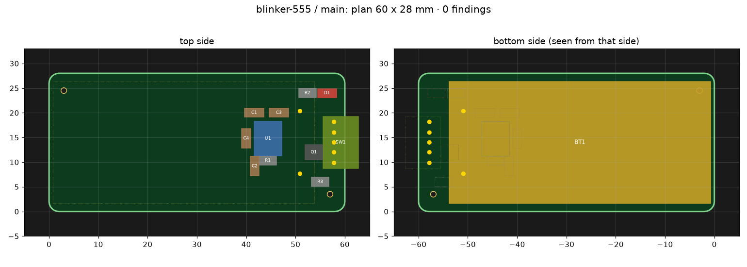
The board file starts with the hand-over's three fixed parts. The plan's frame is mm, origin at the outline's lower left, y up; a part on the bottom is mirrored in its local y (16.3):
revision = "1"
edge_ok = ["SW1"]          # its knob reaches over the right edge

[outline]                  # about the holder's size (53.0 × 24.6 mm), with SW1 at the right end
rect = [60, 28]
corner_radius = 2

[place]
BT1 = { x = 50.9, y = 14, rot = 0, side = "bottom" }   # its body 0.7 … 53.8 mm under the board, the PC pins at the right end
SW1 = { x = 57.8, y = 14, rot = 90, side = "top" }     # body flush with the right edge, the knob over it
D1  = { x = 56.5, y = 24, rot = 0, side = "top" }      # beside SW1: on top, where it is seen
KiCad has no auto-layout: edakit pcb place --rest --write places the other nine by airline length (the placement
plan, 7.4), C1 as U1's decoupling next to its V+. It put them around BT1's pins, which are soldered by hand on this
side, so they were moved 5 mm to the left by hand. [routing] hand_solder_keep_mm = 1 keeps other nets' pads that far
from BT1's and SW1's joints (GEO.spacing, D-8):
Routing
edakit pcb apply writes the parts, the outline and the rules into main.kicad_pcb; edakit route all routes with
Freerouting, fills the ground pours with kicad-cli and runs KiCad's DRC with schematic parity:
$ edakit route all
[ 0.0 min] DSN: 10 nets with >= 2 pins, 34 pads, …, 7 via keep-outs at hand-soldered joints (GEO.spacing), …
…
[ 0.2 min] check: 10 nets routed, 76 track pieces, 4 vias; open: 0
…
[ 0.3 min] pours: 2 zones written and filled by kicad-cli
[ 0.3 min] nothing to reload: the KiCad PCB is a file
[ 0.4 min]   DRC: no findings
It took three tries, each closing a gap of the KiCad chain or of the real footprints (13.10). The first route check
found C1 on two of U1's pads: the library's box of the SOIC-8 ended inside its row of pads, and neither pcb place nor
pcb plan saw the overlap. The second found two SMD pads within 1 mm of BT1's pins. The third try's DRC found SW1's
three free pins on a net "unconnected-(SW1-Pad3)" in KiCad's schematic and on none in the PCB.
Silkscreen
edakit silk apply prints the designators, the board label and the texts of the board file – "+" and "−" beside
BT1's pins and "2x AAA 1.5 V" (D-9) – and checks the print on kicad-cli's Gerber files. D1's designator had no room
beside it and got a fixed spot below the LED ([silk] place):
  top: 11 of 11 designators placed, fixed: D1; without room: –
  top: silkscreen on mask openings 0.000 mm² (target 0), picture -> …/silk_main_top.png
  DRC: no findings
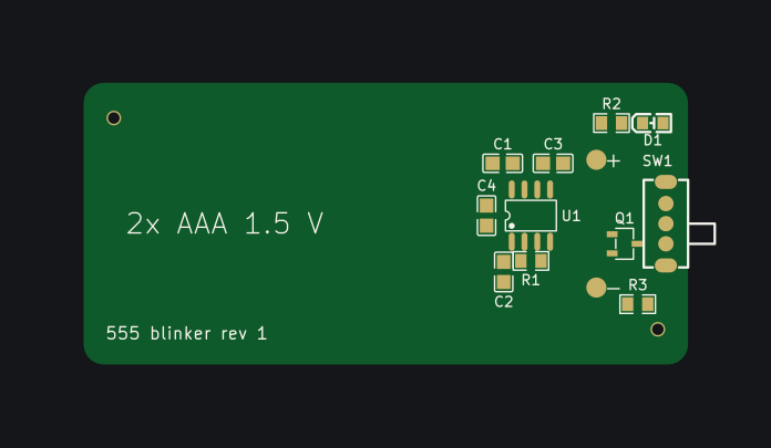
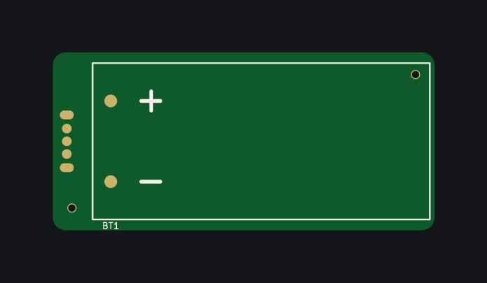
The board as edakit gate --eda draws it from kicad-cli's Gerber files (pictures/board_main_top.png) – the tracks
around U1, the ground pour, mask and silkscreen:
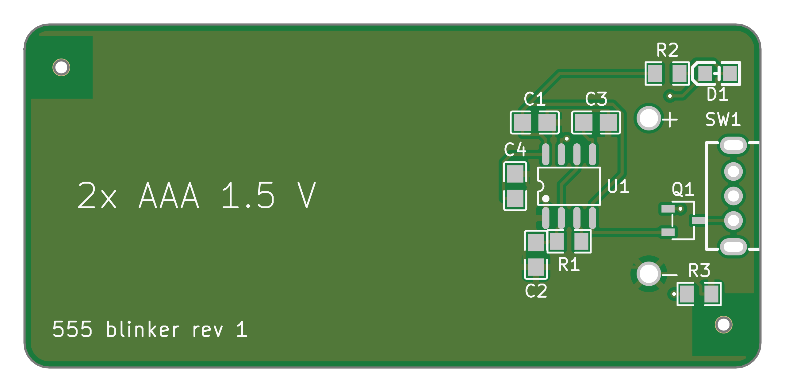
The bottom carries the holder's outline with "+" and "−" from its library footprint. SW1's knob is drawn by its footprint beyond the body and so beyond the outline; GEO.silk's warning on it is accepted in the sign-off file with D-8 – the maker prints nothing there.
The layout review
The layout review M-5 – the agent pcb-reviewer, on a gate run's files – found nothing that blocks and made six notes
(D-10). You chose to build two: tooling holes of your own, which JLCPCB would otherwise drill where it likes, likely on
the empty left of the visible top, with [looks] visible = "top" and a remark for the order form. Routed once more,
Freerouting left two GND pads room for one thermal spoke, which KiCad's DRC counted as starved (13.10). The rest are for
the hand assembly: SW1 before BT1, a dab of glue under the holder's free end, and at M-2 D1's cathode by the chamfer of
its outline:
[tooling]                  # JLCPCB Economic PCBA: two non-plated holes of our own, else JLCPCB drills them where it likes (D-10)
holes = [[57.0, 3.5], [3.0, 24.5]]   # the second under BT1's body: the holder is fitted after the assembly

[looks]
visible = "top"            # the face people see: stage L holds its tracks, vias and texts

[order]
remark = "2 tooling holes added by customer."
18.12 Release
edakit gate --eda runs S, L and F on the KiCad files: SYNC.schematic on kicad-cli's
netlist and ERC, stage L on pcb.json read from the file and KiCad's DRC, stage F on kicad-cli's Gerber, drill and
position files (the gate on KiCad, 16.6).
It took five runs. The first warned about the knob's print and a rounding at BT1's body (13.10); the next waited for M-1 and M-6, then for M-5 on their files; the review's tooling holes gave a new fab hash and M-5 once more. The last:
$ edakit gate --eda
…
[ 0.0 min] step 4/4: L/F board and manufacturing files: main

RELEASED
requirements: 2 passed, 2 open after the export (section 11 of the protocol)
| S Schematic | EasyEDA schematic = graph (parts, LCSC, nets, pins, no-connects) | 1 | 0 | 0 | 0 | 0 | passed |
| L Board | PCB = graph and plan, copper from the Gerber files, DRC, footprints, track widths, holes | 35 | 0 | 1 | 0 | 0 | passed with reservations |
| F Manufacturing | BOM from the graph = EasyEDA, JLCPCB stock, pick and place, Gerber set, outline, manifest | 18 | 0 | 0 | 0 | 0 | passed |
L's warning is the knob's print beyond the outline, accepted with D-8. The run's folder holds what goes to JLCPCB –
fab/main/gerber_main.zip, bom_main.csv, cpl_main.csv, the form's fields in order.md ("Tooling holes: Added by
Customer – 2 x Ø 1.152 mm", "Mark on PCB: Remove Mark") – and fab/polarity_main.png for M-2. edakit export writes
the project's copy:
$ edakit export
[main] -> …/blinker-555/build/edakit/export/main
  schematic_main.pdf                       106 kB
  …
  kicad_main.zip                           57 kB
kicad_main.zip keeps the KiCad project of the release, as an EasyEDA project keeps its .eprj2 (the KiCad project,
16.3).
Order and acceptance. This example ends at RELEASED, no boards ordered: the order is your decision, and chapter 17
shows it. A board of your own goes on with edakit cart prepare (ordering at the manufacturer, 8.4), and M-2 looks at
JLCPCB's assembly preview with polarity_main.png – U1's pin 1, Q1, D1's cathode at the chamfer of its outline.
The hand assembly comes first: SW1, then BT1, its pins trimmed, a dab of glue under its free end (D-10). Then M-4 works through the protocol's acceptance list: BT1 the right way round, D1 blinking while SW1 is on and dark once it is off, and R-2's count – 48 to 72 flashes in 60 s from a lab supply at 3.2 V and at 2.0 V.