Prototype: the bell on a perfboard
A source
This page is a source of edakit – a concept, a prompt or the rules of a session –, shown as it is in the repository. Read it as such; the guides say what edakit does.
Written on 2026-11-09 for the concept perfboard-layout.md, on the owner's request for an example board "damit wir wissen, dass wir vom gleichen reden", and accepted the same day ("jetzt passts"). Its rounds brought the concept's decisions 11 to 23 – straight bridges below and wires on top, the bottom view in the top's orientation, hole names as printed, parts by role, mounting holes in mm, the cut list and the rest –; this version follows all of them and is the reference for the steps LR.1 to LR.4.
Nothing of the steps LR.1 to LR.8 is built. A script does the check and the drawings, as the scripts of footprint-data do; it is no edakit code, and edakit's pytest does not collect it.
| File | What | Stands in for |
|---|---|---|
| bell-perfboard.toml | The plan as text: [perfboard], [place], [near], [[wire]]. It is for the bell's THT circuit (automatic_christmas_bell, variants/tht), whose graph and parts stay unchanged. |
The board file of a hand-wired variant (LR.8) |
| pad-per-hole.toml | The kind as data: pitch, pads, the tolerances for bending leads | LR.1 |
| perfboard.py | Builds the nets the plan makes and compares them with the graph's. Checks the grid, the bodies, the wires, the mounting holes and near, then draws and writes the lists. |
LR.2 to LR.4 |
| bell-perfboard.build.md | Its output: the findings, the cut list, the build list from low to high, the test list for the multimeter and the material | LR.4 |
python3 perfboard.py bell-perfboard.toml <automatic_christmas_bell>/variants/tht
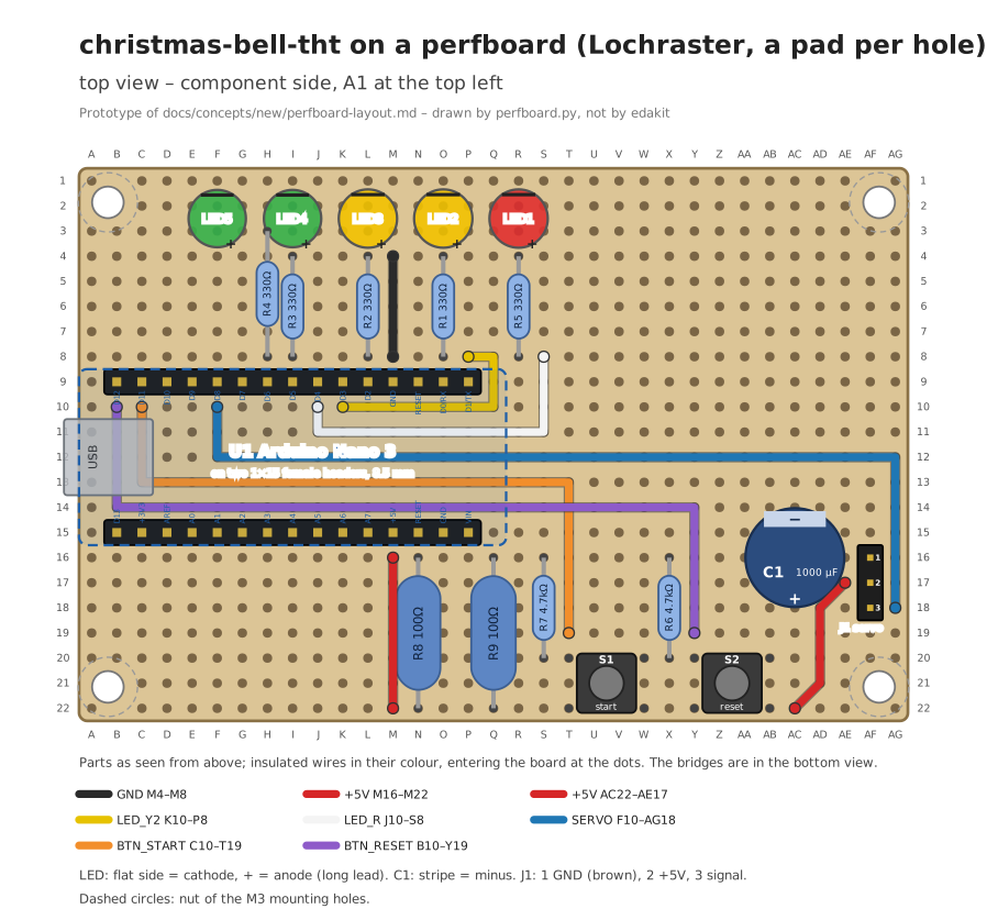
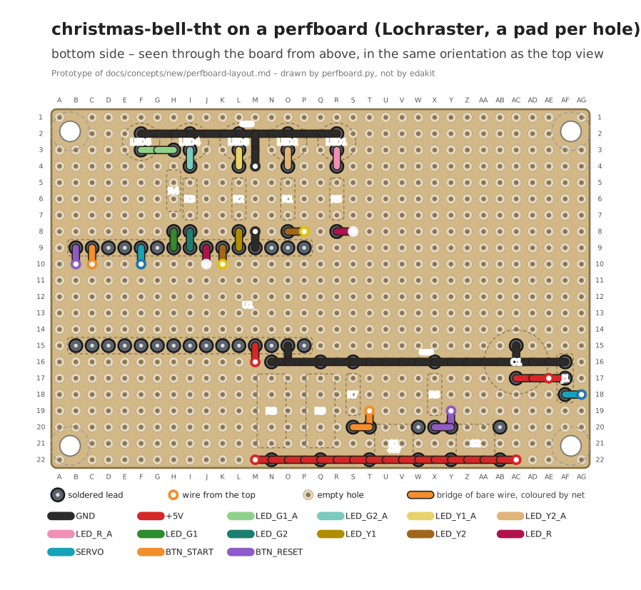
The layout in short
The board is 33 × 22 holes, which is the size of the bell's 85 × 56 mm PCB, cut from a Euro board.
- Nano: on the left with its USB socket at the edge, as on the THT PCB.
- LED row: along the back edge in countdown order (R-13). The cathodes sit in row 2 and are joined by a row of bridges, the anodes in row 3. Each series resistor stands upright below its LED, bridged to the anode above and to the Nano's pin below; R4 stands right above its pin (D6) and reaches row 3, where a straight row of bridges leads to LED5's anode.
- Wires under the Nano: the Nano's pins D6, D5, D4, D3 and D2 carry G1, G2, R, Y2 and Y1, which is not the countdown order G1, G2, Y1, Y2, R. So Y2 and R go as wires on top, under the Nano between its sockets, and come up at its right end. The servo signal and the two button lines take the same way.
- Power: below the Nano, ground runs as a row of bridges along row 16 and +5 V along row 22. R8, R9, the two pull-downs and the buttons stand across or on them; C1 and J1 sit at the right end, C1's plus in J1's row 17. Short wires on top bring +5 V from the Nano's 5V pin down to row 22 and from there around C1 into row 17; another one joins the LED cathodes to the Nano's GND (pin 4).
- In all: 8 insulated wires (445 mm in seven colours) and 76 bridges, every row of them straight. The cut list makes them 17 pieces of bare wire – 11 × 5 mm, 3 × 10 mm, one each of 35, 45 and 50 mm for the rows of cathodes, ground and +5 V –; the 12 bridges beside the wires' ends are the wires' stripped ends.
What the check says
On the plan it finds no error and gives three notes:
- the buttons' leads (6.5 × 4.5 mm) are bent by 0.63 mm into the 7.62 × 5.08 mm grid;
- the LED cathodes reach the rest of ground only inside the Nano (its GND pins 4 and 29). The test list therefore shows ground as two groups that beep together once U1 is plugged in.
A copy of the plan with three typical mistakes: the bridge L8–L9 forgotten, the ground row started one hole too early
(M16 instead of N16, where the +5 V wire comes through), and LED3 the wrong way round (anode = "L2", cathode = "L3"):
error   PERF.short     +5V (9 pins) and GND (12 pins) and LED_Y1_A (LED3.anode in L2) in one piece of copper
error   PERF.short     GND (LED3.cathode in L3) and LED_Y1_A (R2.2 in L4) in one piece of copper
error   PERF.open      GND is open between 12 pins | LED3.cathode in L3
error   PERF.open      LED_Y1 is open between R2.1 in L8 | U1.PD2 in L9
error   PERF.open      LED_Y1_A is open between LED3.anode in L2 | R2.2 in L4
error   PERF.meet      L2 joins GND bridges F2 … R2 with LED3.anode (LED_Y1_A)
error   PERF.meet      L3 joins LED_Y1_A bridge L3–L4 with LED3.cathode (GND)
error   PERF.meet      M16 joins GND bridges M16 … AF16 with +5V bridge M15–M16 with +5V wire M16–M22
PERF.meet names the hole where two nets touch, which is where the soldering iron goes. PERF.corner names the
hole where bridges turn – within a row of them or where two rows end in the same empty hole; the plan's previous
version had three such corners (AC22, AE18/AE17 and H8). The codes PERF.* are the
prototype's own names, not edakit's.
Decided on the prototype
What the first versions left open is decided in the concept (its decisions 11 to 23):
- On the bottom only straight bridges between neighbouring holes; rows of them meet at a lead or in the middle of
another row; everything else is a wire on top, its ends in free holes beside the pins with a bridge below
(11, 16, 17).
PERF.cornerfinds a bridge that turns. - The bottom view in the orientation of the top view, soldered leads clearly marked (12).
- Holes written as the board prints them; the lists say "hole R8" (13).
- Parts with two leads by the holes of their roles, as the LEDs and C1 here (14);
PERF.placefinds leads that do not span the holes named. - Mounting holes in mm, as
[[holes]]of a PCB's board file: here the bell frame's, 78 × 49 mm apart, centred on the board and drilled between the holes (15). - Pins a part joins inside count as one node, through a key
joinedin the parts entry (18) – the script still infers them from the pin name, or on a button from the role. - A module on sockets is raised, and the test list measures without it (19);
nearis the gap between body boxes (20); the bridges are soldered once the leads are in (21). - A cut list with lengths rounded up to 5 mm (22): a straight row of bridges is one piece, a bridge beside a wire's end that wire's stripped end (23).
The values in pad-per-hole.toml are still assumptions without a source: 0.8 mm for bending a lead, 1.5 mm of straight lead for an axial part, no copper rating, and the cut list's allowances (5 mm stripped, 5 mm slack, 1 mm of bare wire beyond the outer pads) – LR.1 takes them from a board's datasheet and a first build.
The prototype does not cover:
- the current per wire and bridge;
- the kind
3-hole-strips; - stage L: the layout hash, the gate and M-5;
- the
[[extra]]items foredakit order; - the hand-over's
edge.
The footprints are a table in the script, not footprint_data or the library cache. near is measured as on a PCB,
the gap between the parts' body boxes.